NCP3066DFSEPGEVB ON Semiconductor, NCP3066DFSEPGEVB Datasheet
NCP3066DFSEPGEVB
Manufacturer Part Number
NCP3066DFSEPGEVB
Description
EVAL BOARD FOR NCP3066DFSEPG
Manufacturer
ON Semiconductor
Specifications of NCP3066DFSEPGEVB
Design Resources
NCP3066 SEPIC DFN Eval Board BOM NCP3066DFSEPGEVB Gerber Files NCP3066 SEPIC DFN Eval Board Schematic
Current - Output / Channel
350mA, 700mA, or 1.05A
Outputs And Type
1, Non-Isolated
Voltage - Output
7.2V
Features
Adjustable peak current limit
Voltage - Input
24.7VAC or 12 ~ 24 VDC
Utilized Ic / Part
NCP3066
Silicon Manufacturer
On Semiconductor
Silicon Core Number
NCP3066
Kit Application Type
Power Management - Voltage Regulator
Rohs Compliant
Yes
Lead Free Status / RoHS Status
Lead free / RoHS Compliant
For Use With/related Products
NCP3066DFSEPG
Other names
NCP3066DFSEPGEVBOS


3/13/2009
Test Procedure for the NCP3066 SEPIC DFN Evaluation Board
1. Connect the input DC voltage between DC input voltage node and DC ground nodes,
2. Place a jumper between DC ground and external enable.
3. Place a removable jumper as shown in Figure 2 as S1 to enable the part, S2 will disable
4. Shorting either S4 or S3 as shown in Figure 1 will place R7 and R6 current sense
5. Set the electronic load to 7.2 V in voltage mode or connect the appropriate LED string.
6. Monitor Iout and ensure the desired output current is 350 mA, 700 mA, or 1.05 A.
ensure the voltage is between 12V and 24V.
the part.
resistors in parallel with R8. The NCP3066 SEPIC demonstration PCB is configured to
output 350 mA when the LED load is set to 7.2 V. Placing one resistor in parallel with
R8 by connecting either S4 or S3 will increase the current to 700 mA. Once the
aforementioned steps are completed, both S4 and S3 will be shorted and the current limit
will increase to 1.05 A.
AC Input1
AC Input2
External Enable
DC Ground
DC Input Voltage
DC Ground
DC Input Voltage
Figure 2: NCP3066 SEPIC DC Input PCB Enable Setup
DC Input PCB Enable Setup and Test
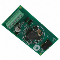
S4
S4
Figure 1: NCP3066 SEPIC PCB
S1
S2
S3
S3
- 1 -
DC Output Ground
DC Output Voltage
DC Output Ground
DC Output Voltage
www.onsemi.com
Related parts for NCP3066DFSEPGEVB
Image
Part Number
Description
Manufacturer
Datasheet
Request
R

Part Number:
Description:
Up to 1.5A Constant Current Switching Regulator
Manufacturer:
ON Semiconductor
Datasheet:

Part Number:
Description:
EVAL BOARD FOR NCP3066SCBCKG
Manufacturer:
ON Semiconductor
Datasheet:

Part Number:
Description:
EVAL BOARD FOR NCP3066SCBSTG
Manufacturer:
ON Semiconductor
Datasheet:

Part Number:
Description:
EVAL BOARD FOR NCP3066S3BCKG
Manufacturer:
ON Semiconductor
Datasheet:
Part Number:
Description:
ON Semiconductor [VOLTAGE REGULATOR]
Manufacturer:
ON Semiconductor
Datasheet:
Part Number:
Description:
357-036-542-201 CARDEDGE 36POS DL .156 BLK LOPRO
Manufacturer:
ON Semiconductor
Datasheet:
Part Number:
Description:
357-036-542-201 CARDEDGE 36POS DL .156 BLK LOPRO
Manufacturer:
ON Semiconductor
Datasheet:
Part Number:
Description:
357-036-542-201 CARDEDGE 36POS DL .156 BLK LOPRO
Manufacturer:
ON Semiconductor
Datasheet:
Part Number:
Description:
357-036-542-201 CARDEDGE 36POS DL .156 BLK LOPRO
Manufacturer:
ON Semiconductor
Datasheet:
Part Number:
Description:
357-036-542-201 CARDEDGE 36POS DL .156 BLK LOPRO
Manufacturer:
ON Semiconductor
Datasheet:
Part Number:
Description:
357-036-542-201 CARDEDGE 36POS DL .156 BLK LOPRO
Manufacturer:
ON Semiconductor
Datasheet:
Part Number:
Description:
357-036-542-201 CARDEDGE 36POS DL .156 BLK LOPRO
Manufacturer:
ON Semiconductor
Datasheet:
Part Number:
Description:
357-036-542-201 CARDEDGE 36POS DL .156 BLK LOPRO
Manufacturer:
ON Semiconductor
Datasheet:
Part Number:
Description:
357-036-542-201 CARDEDGE 36POS DL .156 BLK LOPRO
Manufacturer:
ON Semiconductor
Datasheet:
Part Number:
Description:
357-036-542-201 CARDEDGE 36POS DL .156 BLK LOPRO
Manufacturer:
ON Semiconductor
Datasheet:
NCP3066DFSEPGEVB Summary of contents
Page 1
Test Procedure for the NCP3066 SEPIC DFN Evaluation Board AC Input1 AC Input2 External Enable DC Ground DC Input Voltage DC Ground DC Input Voltage Figure 2: NCP3066 SEPIC DC Input PCB Enable Setup DC Input PCB Enable Setup and ...
Page 2
S4 External Enable DC Ground DC Input Voltage Figure 3: NCP3066 SEPIC DC Input with External Enable Setup DC Input with External Enable Setup 1. Connect the input DC voltage between DC input voltage node and DC ground nodes, ensure ...
Page 3
Shorting either shown in Figure 1 will place R7 and R6 current sense resistors in parallel with R8. The NCP3066 SEPIC demonstration PCB is configured to output 350 mA when the LED load is set ...