NCP3066S3BCKGEVB ON Semiconductor, NCP3066S3BCKGEVB Datasheet - Page 4
NCP3066S3BCKGEVB
Manufacturer Part Number
NCP3066S3BCKGEVB
Description
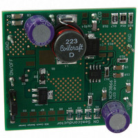
EVAL BOARD FOR NCP3066S3BCKG
Manufacturer
ON Semiconductor
Specifications of NCP3066S3BCKGEVB
Design Resources
NCP3066 Buck EVB BOM NCP3066S3BCKGEVB Gerber Files NCPBUCK 3A EVB Schematic
Current - Output / Channel
3A
Outputs And Type
1, Non-Isolated
Voltage - Output
3.2V
Features
Brightness Control
Voltage - Input
12 ~ 35 V
Utilized Ic / Part
NCP3066
Silicon Manufacturer
On Semiconductor
Silicon Core Number
NCP3066
Kit Application Type
Power Management - Voltage Regulator
Rohs Compliant
Yes
Lead Free Status / RoHS Status
Lead free / RoHS Compliant
For Use With/related Products
NCP3066S3BCKG
Other names
NCP3066S3BCKGEVBOS


6. Low duty cycle pulse techniques are used during test to maintain junction temperature as close to ambient temperature as possible.
7. The V
8. NCV prefix is for automotive and other applications requiring site and change control and extended operating temperature conditions.
ELECTRICAL CHARACTERISTICS
otherwise specified)
OSCILLATOR
OUTPUT SWITCH (Note 6)
V
COMPARATOR
ON/OFF FEATURE
TOTAL DEVICE
I
DISCHG
V
SWCE(DROP)
REG
T
T
Symbol
depends on comparator response time and di/dt current slope. See the Operating Description section for details.
IPK(Sense)
I
I
DISCHG
SHDHYS
ON_MIN
C(OFF)
I
T
I
f
I
STBY
V
CHG
CII in
OSC
V
I
V
I
SHD
I
CC
IH
TH
IL
IH
IL
LiNE
/I
IPK
CHG
(Sense) Current Limit Sense Voltage is specified at static conditions. In dynamic operation the sensed current turn−off value
Frequency
Discharge to Charge Current Ratio
Capacitor Discharging Current
Capacitor Charging Current
Current Limit Sense Voltage
Darlington Switch Collector to
Emitter Voltage Drop
Collector Off−State Current
Threshold Voltage
Threshold Voltage Line Regulation
Input Bias Current
ON/OFF Pin Logic Input Level High
V
ON/OFF Pin Logic Input Level Low
V
ON/OFF Pin Input Current
ON/OFF Pin = 5 V (ON)
ON/OFF Pin Input Current
ON/OFF Pin = 0 V (OFF)
ON/OFF Pin Minimum Width
Supply Current
Standby Quiescent Current
Thermal Shutdown Threshold
Hysteresis
OUT
OUT
= 0 V
= Nominal Output Voltage
Characteristic
(V
CC
= 5.0 V, −40°C < T
http://onsemi.com
ON/OFF Pin = 5.0 V (OFF)
V
CT = 2.2 nF, Pin 7 = V
(Pin 7 to V
(Pin 7 to V
(Pin 7 to V
(V
(I
Pin
T
T
SW
(V
(V
remaining pins open)
Pin5
(T
J
J
T
T
J
T
CC
CC
5 > V
= −40°C to +125°C
= −40°C to +125°C
J
J
J
< +125°C for NCV3066, 0°C < T
= 1.0 A, T
J
= 25°C) (Note 7)
(V
= 0°C to +85°C
= 0°C to +85°C
= 0 V, C
4
Conditions
= 0°C to 85°C
T
= 3.0 V to 40 V)
T
(V
T
T
T
T
= 5.0 V to 40 V,
T
J
CE
J
(Note 6)
J
J
J
J
J
J
th
in
= 25°C
= 25°C)
CC
CC
CC
= 25°C
= 25°C
= 25°C
= 25°C
= 25°C
= 25°C
, Pin 2 = GND,
= 40 V)
= V
, T
, T
, T
T
J
th
J
J
J
= 2.2 nF,
= 25°C)
)
= 25°C)
= 25°C)
= 25°C)
CC
,
−1000
−10%
−5%
−6.0
Min
110
165
5.5
2.2
2.4
−
−
J
< +85°C for NCP3066 unless
1650
−100
Typ
150
275
200
235
235
235
160
6.0
1.0
1.0
2.0
1.0
15
50
85
10
−
−
−
−
+10%
1000
Max
+5%
190
235
120
120
6.5
1.3
6.0
1.0
0.8
7.0
10
−
−
Unit
kHz
mV
mV
mV
mA
mA
mA
mA
nA
mA
mA
mA
ms
°C
°C
V
V
V
−
Related parts for NCP3066S3BCKGEVB
Image
Part Number
Description
Manufacturer
Datasheet
Request
R

Part Number:
Description:
Up to 1.5A Constant Current Switching Regulator
Manufacturer:
ON Semiconductor
Datasheet:

Part Number:
Description:
EVAL BOARD FOR NCP3066DFSEPG
Manufacturer:
ON Semiconductor
Datasheet:

Part Number:
Description:
EVAL BOARD FOR NCP3066SCBCKG
Manufacturer:
ON Semiconductor
Datasheet:

Part Number:
Description:
EVAL BOARD FOR NCP3066SCBSTG
Manufacturer:
ON Semiconductor
Datasheet:
Part Number:
Description:
ON Semiconductor [VOLTAGE REGULATOR]
Manufacturer:
ON Semiconductor
Datasheet:
Part Number:
Description:
357-036-542-201 CARDEDGE 36POS DL .156 BLK LOPRO
Manufacturer:
ON Semiconductor
Datasheet:
Part Number:
Description:
357-036-542-201 CARDEDGE 36POS DL .156 BLK LOPRO
Manufacturer:
ON Semiconductor
Datasheet:
Part Number:
Description:
357-036-542-201 CARDEDGE 36POS DL .156 BLK LOPRO
Manufacturer:
ON Semiconductor
Datasheet:
Part Number:
Description:
357-036-542-201 CARDEDGE 36POS DL .156 BLK LOPRO
Manufacturer:
ON Semiconductor
Datasheet:
Part Number:
Description:
357-036-542-201 CARDEDGE 36POS DL .156 BLK LOPRO
Manufacturer:
ON Semiconductor
Datasheet:
Part Number:
Description:
357-036-542-201 CARDEDGE 36POS DL .156 BLK LOPRO
Manufacturer:
ON Semiconductor
Datasheet:
Part Number:
Description:
357-036-542-201 CARDEDGE 36POS DL .156 BLK LOPRO
Manufacturer:
ON Semiconductor
Datasheet:
Part Number:
Description:
357-036-542-201 CARDEDGE 36POS DL .156 BLK LOPRO
Manufacturer:
ON Semiconductor
Datasheet:
Part Number:
Description:
357-036-542-201 CARDEDGE 36POS DL .156 BLK LOPRO
Manufacturer:
ON Semiconductor
Datasheet:
Part Number:
Description:
357-036-542-201 CARDEDGE 36POS DL .156 BLK LOPRO
Manufacturer:
ON Semiconductor
Datasheet: