NCP5030MTTXGEVB ON Semiconductor, NCP5030MTTXGEVB Datasheet - Page 2
NCP5030MTTXGEVB
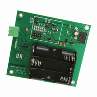
Manufacturer Part Number
NCP5030MTTXGEVB
Description
EVAL BOARD FOR NCP5030MTTXG
Manufacturer
ON Semiconductor
Datasheets
1.NCP5030MTTXG.pdf
(14 pages)
2.NCP5030MTTXGEVB.pdf
(1 pages)
3.NCP5030MTTXGEVB.pdf
(7 pages)
Specifications of NCP5030MTTXGEVB
Design Resources
NCP5030MTTXG EVB BOM NCP5030MTTXGEVB Gerber Files NCP5030MTTXG EVB Schematic
Current - Output / Channel
900mA
Outputs And Type
1, Non-Isolated
Voltage - Output
2.2 ~ 5.5 V
Features
Adjustable
Voltage - Input
2.7 ~ 5.5V
Utilized Ic / Part
NCP5030
Rohs Compliant
NO
Lead Free Status / RoHS Status
Lead free / RoHS Compliant
For Use With/related Products
NCP5030MTTXG
Other names
NCP5030MTTXGEVBOS


Operation
VLF5014A4R7M1R1 is recommended at output current
under 500 mA, and RLF7030T4R7M3R4 is recommended
when output current is larger than 700 mA.
5.5 V. Maximum input voltage is 7.0 V and maximum
continuous output current is 900 mA.
Current Setting Selection
connected between FB pin and GND. R102 to R106 and
J109 are used for output current setting according to eq. 1:
Table 1. Input Power Connector
Table 2. Output Power Connector
Table 3. Jumper Setup
Table 4. Test Points
L101 selection depends on the output current,
The power supply of NCP5030 should be from 2.7 V to
The output is determined by the resistor or resistors
J108−1/2
J108−5/6
J102−1/2
J102−2/3
Symbol
J101−1
J101−2
J107−1
J107−2
TP101
TP102
TP103
TP104
J103
J110
J104
J105
J109
J111
I out (A) + 0.2
Positive terminal of external power supply
GND of external power supply
Positive terminal of 3*AA batteries in serial
GND of 3*AA batteries in serial
VOUT of NCP5030
FB of NCP5030
Peak current set to about 3 A, peak current and setting resistor selection can reference the datasheet of
NCP5030
Peak current set to about 1.5 A, peak current and setting resistor selection can reference the datasheet of
NCP5030
Short will connect CTRL to PVIN and enable NCP5030
GND test jumper
Must be connected to ensure NCP5030 work properly, can measure inductor current here, such as peak
current of inductor
Select D101 as load of NCP5030, be careful if J111 or J108 is connected
Select D102 as load of NCP5030, be careful if J105 or J108 is connected
Output current setting, reference to table 5(Output current setting table)
CTRL and enable of NCP5030.
FB, feedback, reference voltage is 200 mV.
Switch LX1
Switch LX2
R(W)
(eq. 1)
http://onsemi.com
2
CAUTION:
J109 allows parallel connections of several resistors to select
output current.
(1 = short connected; 0 = left open)
Where R is the total resistance between FB and GND,
Following is the output current setting table of J109
Descriptions
1. Exceeding the maximum input voltage may
2. Too long time duration at over output current
damage NCP5030 permanently!
may decrease LED life time or even damage
LED!
Related parts for NCP5030MTTXGEVB
Image
Part Number
Description
Manufacturer
Datasheet
Request
R

Part Number:
Description:
ON Semiconductor [VOLTAGE REGULATOR]
Manufacturer:
ON Semiconductor
Datasheet:
Part Number:
Description:
357-036-542-201 CARDEDGE 36POS DL .156 BLK LOPRO
Manufacturer:
ON Semiconductor
Datasheet:
Part Number:
Description:
357-036-542-201 CARDEDGE 36POS DL .156 BLK LOPRO
Manufacturer:
ON Semiconductor
Datasheet:
Part Number:
Description:
357-036-542-201 CARDEDGE 36POS DL .156 BLK LOPRO
Manufacturer:
ON Semiconductor
Datasheet:
Part Number:
Description:
357-036-542-201 CARDEDGE 36POS DL .156 BLK LOPRO
Manufacturer:
ON Semiconductor
Datasheet:
Part Number:
Description:
357-036-542-201 CARDEDGE 36POS DL .156 BLK LOPRO
Manufacturer:
ON Semiconductor
Datasheet:
Part Number:
Description:
357-036-542-201 CARDEDGE 36POS DL .156 BLK LOPRO
Manufacturer:
ON Semiconductor
Datasheet:
Part Number:
Description:
357-036-542-201 CARDEDGE 36POS DL .156 BLK LOPRO
Manufacturer:
ON Semiconductor
Datasheet:
Part Number:
Description:
357-036-542-201 CARDEDGE 36POS DL .156 BLK LOPRO
Manufacturer:
ON Semiconductor
Datasheet:
Part Number:
Description:
357-036-542-201 CARDEDGE 36POS DL .156 BLK LOPRO
Manufacturer:
ON Semiconductor
Datasheet:
Part Number:
Description:
357-036-542-201 CARDEDGE 36POS DL .156 BLK LOPRO
Manufacturer:
ON Semiconductor
Datasheet:
Part Number:
Description:
Manufacturer:
ON Semiconductor
Datasheet:
Part Number:
Description:
Manufacturer:
ON Semiconductor
Datasheet:
Part Number:
Description:
Manufacturer:
ON Semiconductor
Datasheet: