IRPLLED1 International Rectifier, IRPLLED1 Datasheet
IRPLLED1
Specifications of IRPLLED1


Related parts for IRPLLED1

IRPLLED1 Summary of contents
Page 1
... IRPLLED1 350mA to 1.5A High Voltage LED Driver 1. Introduction………………………………………………………………...….1 2. Constant Current Control.......................................................................3 3. Frequency Selection..............................................................................6 4. Output L1 and COUT Selection .............................................................6 5. MOSFET vs Diode for the low side switch.… ...
Page 2
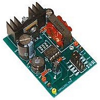
... LEDs, dimming and appropriate fault protections. The IRS2540/1 is specifically designed to address these requirements The IRPLLED1evaluation board is a high voltage LED driver designed to operate from a DC input voltage of 50V to 170V and produce an output voltage of 16V-24V to supply a programmable load current of 350mA, 700mA, 1A ...
Page 3
Constant current control The IRS2540 time-delayed hysteretic Buck controller. During normal operating conditions the output current is regulated via the IFB pin voltage to a nominal value of 500mV. This feedback signal is compared to an internal ...
Page 4
Fig. 3 IRS2540/1 Control Signals, Iavg=1.2A The switching continues to regulate the current at an average value determined as follows: when the output combination of L1 and COUT is large enough to maintain a low ripple on IFB (less than ...
Page 5
Since some of these equivalent values of resistance are not available, series and parallel combinations are used and are specified as follows (all combinations use standard value resistors: 1.43Ω, 0.56Ω, and 0.47Ω): = 43 Ω 350mA = ...
Page 6
Fig. 6 Vbus = 100V 470uH, COUT = 33uF 3. Frequency selection The frequency in the IRS2540/1 application is free running and maintains current regulation by quickly adapting ...
Page 7
Fig. 7 Iout = 350mA, Vout = 16.8V, COUT = 0uF 400 390 380 370 360 350 340 330 30 Fig. 8 Iout = 350mA, Vout = 16.8V, COUT = 0uF www.irf.com 80 ...
Page 8
Fig. 9 Iout = 350mA, Vin = 50V, COUT = 0uF 345 343 341 339 337 335 333 331 329 327 325 13 Fig. 10 Iout = 350mA, ...
Page 9
The output capacitor can be used simultaneously to reduce the frequency and improve current control accuracy. Fig. 11 shows how the capacitance reduces the frequency over a range of input voltage. A small capacitance of 4.7uF has a large effect ...
Page 10
Fig. 13 Iout = 350mA, Vout = 16.8V 470uH The addition of the COUT is essentially increasing the amount of energy that can be stored in the output ...
Page 11
Fig. 15 Iout = 350mA, Vin = 100V, Vout = 16.85V 470uH, COUT = 33uF L1 and COUT need to be chosen so that enough energy is stored to supply the load during t_HO_on while maintaining current control ...
Page 12
VBUS L 2 ROV CBUS1 CBUS2 ROV 2 COM EN Fig. 16 Alternate IRS2540/1 Time-Delayed Hysteretic Controlled Evaluation Board Schematic Note: Rout is needed only in few applications The reverse recovery problem is incurred during the deadtime after the low ...
Page 13
Fig. 17 Using a low side FET, Vin = 100V, Iout = 1.5A, Vout = 17V Fig. 18 Using a diode on the low side, Vin = 100V, Iout = 1.5A, Vout = 17V www.irf.com RD-0608 13 ...
Page 14
Fig. 19 Low side FET vs. low side diode comparison, Vin = 100V, Iout = 1.5A, Vout = 17V Fig. 20 Low side FET and low side diode comparison, Vin = 100V, Iout = 1.5A, Vout = 17V The bus ...
Page 15
A detailed evaluation of system needs and cost should be performed prior to choosing a MOSFET or diode for the low side. Although a diode is cheaper, in certain cases the associated power losses may require a heatsink, nullifying the ...
Page 16
RS1 ( ) 2 − Bus = max − 14 − 170 14 V Bus = = 1 max RS 1 ...
Page 17
During an open circuit condition, without the watchdog timer, the HO output would remain high at all times and the charge stored in the bootstrap capacitor (CBOOT) would slowly leak until reaching zero, thus eliminating the floating power supply for ...
Page 18
... The following circuit is a simple enable pin dimming signal generator. VBUS COM Fig. 22 Suggested PWM Driver (not included in IRPLLED1.5X2 external supply for VCC is used, the minimum amount of dimming achievable (light output approaches 0%) will be determined by the “on” time of the HO output, when in a fully functional regulating state. To maintain reliable dimming recommended to keep the “ ...
Page 19
... This current spike stresses the load possibly decreasing LED operating lifetime. The IRPLLED1includes a jumper setting to define whether or not the board is being used in the dimming mode. This two position jumper allows the designer to either include or exclude the resistor Rout, which is in series with the output capacitor ...
Page 20
Fig. 25 Load Current Spike Excluding Rout Fig. 26 Load Current Ripple Excluding Rout www.irf.com Iout = 350mA, Vin = 100V, Vout = 17V Iout = 350mA, Vin = 100V, Vout = 17V RD-0608 20 ...
Page 21
... PWM dimming signal will still be the dominant factor of the overall output current regulation capabilities. It should be noted that the IRPLLED1 reference design board reflects the schematic of Figure 16 where a high speed diode is used in place of the lower MOSFET switch indicated in Figure 1. ...
Page 22
HO cycle as shown in the waveform diagram below. The reason for this is to avoid the possibility off ENN transitioning from low to high at the exact time that HO transitions from low ...
Page 23
The open load protection circuit in Fig 29 is recommended for isolated non-dimming applications where the load may be disconnected and then reconnected without shutting down the driver. When the load is reconnected with power on this would reduce the ...
Page 24
out − = out ...
Page 25
... EMC performance The IRPLLED1 evaluation board has not been EMC tested. Input and Output filters can be used to reduce the conducted emissions to below the limits of the applicable EMC standard as needed. Inductors may require a powdered Iron core rather than Ferrite, it can handle a much larger current before saturating. If EMC is of critical importance, it may be beneficial to use a MOSFET for the upper switching element and a diode for the lower switch ...
Page 26
Bill of Materials Device Item Description Type 1 C 10uF, 25V, Radial 2 C 100nF, 200V, 1812 3 C 100nF, 50V, 0805 4 C 33uF, 100V 5 C 1nF, 50V, 0805 6 C 47uF, 200V 7 D 200V, 1A ...
Page 27
Enable Signal Generator (not included) Device Item Description Type 1 C 10uF, 25V, Radial ECEA1EKG100 2 C 100nF, 50V, 0805 VJ0805Y104KXATW1BC 3 C 1nF, 50V, 0805 VJ0805Y102KXACW1BC 4 D Mini Melf LL4148 5 R 1k, 1%, 0805 MRC10EZHF1001 6 R ...
Page 28
Bottom Overlay www.irf.com Bottom Metal RD-0608 28 ...
Page 29
Revision History Rev/Date Change Description Updated Figure 16 to provide exact schematic of the demo board including sync modification. Added Figure 4a to show LED current jumper settings. Rev 2. Correction made to duty cycle calculation in section 8. Aug ...