LM3500TL-16EV National Semiconductor, LM3500TL-16EV Datasheet - Page 5
LM3500TL-16EV
Manufacturer Part Number
LM3500TL-16EV
Description
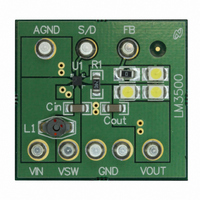
BOARD EVALUATION LM3500TL-16
Manufacturer
National Semiconductor
Series
PowerWise®r
Specifications of LM3500TL-16EV
Current - Output / Channel
20mA
Outputs And Type
1, Non-Isolated
Voltage - Output
14V
Features
Shutdown
Voltage - Input
2.7 ~ 5.5 V
Utilized Ic / Part
LM3500
Core Chip
LM3500
Topology
Buck
No. Of Outputs
1
Output Voltage
16V
Input Voltage
2.7V To 7V
Kit Contents
Board
Development Tool Type
Hardware - Eval/Demo Board
Lead Free Status / RoHS Status
Not applicable / Not applicable


I
I
SHDN
Threshold
Vout
VL
Symbol
Note 1: Absolute maximum ratings are limits beyond which damage to the device may occur. Operating Ratings are conditions for which the device is intended
to be functional, but device parameter specifications may not be guaranteed. For guaranteed specifications and test conditions, see the Electrical Characteristics.
Note 2: This condition applies if V
Note 3: For more detailed soldering information and specifications, please refer to National Semiconductor Application Note 1112: Micro SMD Wafer Level Chip
Scale Package (AN-1112), available at www.national.com.
Note 4: The human body model is a 100 pF capacitor discharged through a 1.5 kΩ resistor into each pin. The machine model is a 200 pF capacitor discharged
directly into each pin.
Note 5: In applications where high power dissipation and/or poor package thermal resistance is present, the maximum ambient temperature may have to be
derated. Maximum ambient temperature (T
dissipation of the device in the application (P
following equation: T
Note 6: Junction-to-ambient thermal resistance (θ
test board conforming to JEDEC standards. In applications where high maximum power dissipation exists, special care must be paid to thermal dissipation issues
when designing the board layout.
Note 7: All limits guaranteed at room temperature (standard typeface) and at temperature extremes (bold typeface). All room temperature limits are production
tested, guaranteed through statistical analysis or guaranteed by design. All limits at temperature extremes are guaranteed via correlation using standard Statistical
Quality Control (SQC) methods. All limits are used to calculate Average Outgoing Quality Level (AOQL).
Note 8: Typical numbers are at 25°C and represent the most likely norm.
Note 9: Feedback current flows out of the pin.
Note 10: Current flows into the pin.
Typical Performance Characteristics
V
(LM3500-16)
V
(LM3500-21)
PMOS Switch Leakage
Current (LM3500-16)
PMOS Switch Leakage
Current (LM3500-21)
SHDN Low
SHDN High
Switching Quiescent Current vs V
OUT
OUT
A-MAX
Bias Current
Bias Current
= T
Parameter
J-MAX-OP
IN
< V
– (θ
OUT
JA
A-MAX
. If V
× P
D-MAX
IN
D-MAX
) is dependent on the maximum operating junction temperature (T
> V
), and the junction-to ambient thermal resistance of the part/package in the application (θ
JA
) is highly application and board-layout dependent. The 75ºC/W figure provided was measured on a 4-layer
).
OUT
V
V
V
V
OUT
OUT
OUT
OUT
, a voltage greater than V
20065755
= 15V, SHDN = V
= 20V, SHDN = V
= 15V, V
= 20V, V
IN
Conditions
SW
SW
= 0V
= 0V
5
IN
IN
IN
+ 0.3V should not be applied to the V
Non-Switching Quiescent Current vs V
(Note 7)
Min
1.1
(Note 8)
J-MAX-OP
0.01
0.01
0.65
0.65
Typ
260
300
OUT
= 125ºC), the maximum power
or V
SW
(Note 7)
pins.
Max
400
460
0.3
3
3
JA
20065756
), as given by the
IN
www.national.com
Units
µA
µA
V
Related parts for LM3500TL-16EV
Image
Part Number
Description
Manufacturer
Datasheet
Request
R

Part Number:
Description:
IC LED DRVR WHT BCKLT 8-MICROSMD
Manufacturer:
National Semiconductor
Datasheet:
Part Number:
Description:
IC LED DRVR WHT BCKLT 8-MICROSMD
Manufacturer:
National Semiconductor
Datasheet:

Part Number:
Description:
Synchronous Step-up DC/DC Converter For White Led Applicationsthe LM3500 is a Fixed Frequency Synchronous Step-up DC/DC Converter in a Small 8-bump Thin Micro SMD Package. The LM3500 is Ideal For White Led Applications For Cellular Phone Back-lightin
Manufacturer:
National Semiconductor Corporation

Part Number:
Description:
LM3500 Synchronous Step-up DC/DC Converter for White LED Applications; Package: MICRO SMD; No of Pins: 8; Qty per Container: 250; Container: Reel
Manufacturer:
National Semiconductor
Datasheet:

Part Number:
Description:
The LM350 is an adjustable 3-terminal positive voltage regulator capable of supplying in excess of 3
Manufacturer:
Fairchild Semiconductor
Datasheet:

Part Number:
Description:
3.0 A, Adjustable Output, Positive Voltage Regulat
Manufacturer:
On Semiconductor
Part Number:
Description:
National Semiconductor [8-Bit D/A Converter]
Manufacturer:
National Semiconductor
Datasheet:
Part Number:
Description:
National Semiconductor [Media Coprocessor]
Manufacturer:
National Semiconductor
Datasheet:
Part Number:
Description:
Digitally Controlled Tone and Volume Circuit with Stereo Audio Power Amplifier, Microphone Preamp Stage and National 3D Sound
Manufacturer:
National Semiconductor
Datasheet:
Part Number:
Description:
Digitally Controlled Tone and Volume Circuit with Stereo Audio Power Amplifier, Microphone Preamp Stage and National 3D Sound
Manufacturer:
National Semiconductor
Datasheet:
Part Number:
Description:
AC97 Rev 2 Codec with Sample Rate Conversion and National 3D Sound
Manufacturer:
National Semiconductor
Part Number:
Description:
Manufacturer:
National Semiconductor
Datasheet:
Part Number:
Description:
Manufacturer:
National Semiconductor
Datasheet: