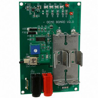
NCP5603GEVB ON Semiconductor, NCP5603GEVB Datasheet

NCP5603GEVB
Specifications of NCP5603GEVB
Related parts for NCP5603GEVB
NCP5603GEVB Summary of contents
Page 1
NCP5603 High Efficiency Charge Pump Converter The NCP5603 is an integrated circuit dedicated to the medium power White LED applications. The power conversion is achieved by means of a charge pump structure, using two external ceramic capacitors, making the system ...
Page 2
V bat GND bat 4.7 mF/ C1P C1 1 mF/ C1N 6 EN/PWM PWM 4 Fsel FSEL 5 VSEL Vsel 8 GND GND Figure 1. Typical Application NCP5603 7 C2N C4 10 ...
Page 3
V bat 3 V bat Thermal Shutdown V bat 4 Fsel 5 Vsel 6 EN NCP5603 V bat GND V bat GND BANDGAP Figure 2. Block Diagram http://onsemi.com 3 10 C2P 7 C2N 9 C1N 2 C1P V out 1 ...
Page 4
PIN FUNCTION DESCRIPTION Pin Symbol Type 1 V OUTPUT, PWR out 2 C1N POWER 3 V POWER bat 4 Fsel INPUT, Digital 5 Vsel INPUT, Digital 6 EN/PWM INPUT, Digital 7 C2N POWER 8 GND GROUND 9 C1P POWER 10 ...
Page 5
MAXIMUM RATINGS Rating Power Supply Voltage Power Supply Current Digital Input Pins Digital Input Pins Output Voltage ESD Capability (Note 3) Human Body Model Machine Model DFN10, 3x3 Package Power Dissipation @ Tamb = +85°C Thermal Resistance, Junction-to-Air (R Operating ...
Page 6
ELECTRICAL CHARACTERISTICS Characteristic Power Supply = 0 mA Quiescent Current @ bat out @ Pulsed Clock Fop = 262 kHz @ Pulsed Clock Fop = 650 kHz @ Continuous Clock Fop = 262 kHz @ ...
Page 7
I = 120 mA OUT 2.5 3.0 3.5 4.0 V (V) in Figure 3. Operating Modes Transitions and Output Power Efficiency @ V out 100 I = 160 mA OUT -40°C 90 25°C 80 ...
Page 8
TYPICAL CHARACTERISTICS Test conditions 25mA LED Figure 9. Typical PWM Dimming mF/ mF/6.3 V GND EN PWR-FLASH FSEL GND VSEL Figure 10. Typical High Power Flash Circuit NCP5603 = 3.6 ...
Page 9
Table 1. Ceramic Preferred Capacitors Manufacturer TDK TDK TDK NCP5603 2 4.5 V out FSEL ...
Page 10
TP2 C3 1 1.0 mF/ SENSE R9 D4 TP1 82 W LW67C out 82 W LW67C LW67C LW67C C2 1 mF/ mF/16 V ...
Page 11
NCP5603 Figure 13. Evaluation Board: Silk View (Top View) http://onsemi.com 11 ...
Page 12
... Side View (Optional) 2.1746 10X 0.5651 10X 0.3008 *For additional information on our Pb-Free strategy and soldering details, please download the ON Semiconductor Soldering and Mounting Techniques Reference Manual, SOLDERRM/D. http://onsemi.com 12 NOTES: 1. DIMENSIONING AND TOLERANCING PER ASME Y14.5M, 1994. 2. CONTROLLING DIMENSION: MILLIMETERS. ...
Page 13
... Opportunity/Affirmative Action Employer. This literature is subject to all applicable copyright laws and is not for resale in any manner. PUBLICATION ORDERING INFORMATION LITERATURE FULFILLMENT: Literature Distribution Center for ON Semiconductor P.O. Box 5163, Denver, Colorado 80217 USA Phone: 303-675-2175 or 800-344-3860 Toll Free USA/Canada Fax: 303-675-2176 or 800-344-3867 Toll Free USA/Canada ...


