NCP5050GEVB ON Semiconductor, NCP5050GEVB Datasheet - Page 4
NCP5050GEVB
Manufacturer Part Number
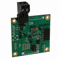
NCP5050GEVB
Description
EVAL BOARD FOR NCP5050G
Manufacturer
ON Semiconductor
Specifications of NCP5050GEVB
Design Resources
NCP5050 EVB BOM NCP5050 EVB Schematic NCP5050GEVB Gerber Files
Current - Output / Channel
Adjustable
Outputs And Type
1, Non-Isolated
Voltage - Output
Up to 20V
Features
Dimmable
Voltage - Input
2.7 ~ 5.5 V
Utilized Ic / Part
NCP5050
Core Chip
NCP5050
Topology
Boost
No. Of Outputs
1
Dimming Control Type
PWM
Development Tool Type
Hardware - Eval/Demo Board
Leaded Process Compatible
Yes
Mcu Supported Families
NCP5050
Rohs Compliant
Yes
Lead Free Status / RoHS Status
Lead free / RoHS Compliant
For Use With/related Products
NCP5050G
Other names
NCP5050GEVBOS


Stresses exceeding Maximum Ratings may damage the device. Maximum Ratings are stress ratings only. Functional operation above the
Recommended Operating Conditions is not implied. Extended exposure to stresses above the Recommended Operating Conditions may affect
device reliability.
1. Maximum electrical ratings are defined as those values beyond which damage to the device may occur at T
2. According to JEDEC standard JESD22−A108B.
3. This device series contains ESD protection and passes the following tests:
4. Latch up Current Maximum Rating: $100 mA per JEDEC standard: JESD78.
5. The thermal shutdown set to 160°C (typical) avoids irreversible damage on the device due to power dissipation.
6. For the 10−Pin 3x3 WDFN Package, the R
7. Per IPC/JEDEC standard: J−STD−020A.
8. The maximum package power dissipation limit must not be exceeded.
MAXIMUM RATINGS
P
Power Supply Voltage (Note 2)
Over Voltage Protection
Human Body Model (HBM) ESD Rating (Note 3)
HCS and FB Pins
Machine Model (MM) ESD Rating (Note 3)
HCS and FB Pins
Digital Input Voltage
Digital Input Current
WDFN 3x3 Package
Power Dissipation @ T
Thermal Resistance, Junction−to−Case
Thermal Resistance, Junction−to−Air
Operating Ambient Temperature Range
Operating Junction Temperature Range
Maximum Junction Temperature
Storage Temperature Range
Moisture Sensitivity Level (Note 7)
Human Body Model (HBM) per JEDEC standard: JESD22−A114 for all pins.
Machine Model (MM) per JEDEC standard: JESD22−A115 for all pins.
board having 51 mm
d
+
125 * T
R
qJA
A
2
A
dissipation area on circuit side and board size ground plane on other side.
(Note 1)
= +85°C
Rating
qJA
is highly dependent on the PCB heat−sink area. For example, R
http://onsemi.com
4
CTRL, CM
ESD HBM
ESD MM
Symbol
T
R
R
MSL
P
JMAX
T
V
P
T
T
qJC
qJA
stg
Vin
A
S
D
J
−0.3 < V
−10 to +125
−65 to +150
−10 to +85
(Note 5)
(Note 6)
Value
in
+150
2000
1000
200
150
7.0
1.0
25
10
< V
1
qJA
bat
A
= 25°C.
+ 0.3
can be 61°C/W for 2 layers
°C/W
Unit
mA
°C
°C
°C
°C
W
V
V
V
V
V
Related parts for NCP5050GEVB
Image
Part Number
Description
Manufacturer
Datasheet
Request
R

Part Number:
Description:
4.5 W Inductive Boost Led Driver For Flash And Lcd Backlight
Manufacturer:
ON Semiconductor
Datasheet:
Part Number:
Description:
ON Semiconductor [VOLTAGE REGULATOR]
Manufacturer:
ON Semiconductor
Datasheet:
Part Number:
Description:
357-036-542-201 CARDEDGE 36POS DL .156 BLK LOPRO
Manufacturer:
ON Semiconductor
Datasheet:
Part Number:
Description:
357-036-542-201 CARDEDGE 36POS DL .156 BLK LOPRO
Manufacturer:
ON Semiconductor
Datasheet:
Part Number:
Description:
357-036-542-201 CARDEDGE 36POS DL .156 BLK LOPRO
Manufacturer:
ON Semiconductor
Datasheet:
Part Number:
Description:
357-036-542-201 CARDEDGE 36POS DL .156 BLK LOPRO
Manufacturer:
ON Semiconductor
Datasheet:
Part Number:
Description:
357-036-542-201 CARDEDGE 36POS DL .156 BLK LOPRO
Manufacturer:
ON Semiconductor
Datasheet:
Part Number:
Description:
357-036-542-201 CARDEDGE 36POS DL .156 BLK LOPRO
Manufacturer:
ON Semiconductor
Datasheet:
Part Number:
Description:
357-036-542-201 CARDEDGE 36POS DL .156 BLK LOPRO
Manufacturer:
ON Semiconductor
Datasheet:
Part Number:
Description:
357-036-542-201 CARDEDGE 36POS DL .156 BLK LOPRO
Manufacturer:
ON Semiconductor
Datasheet:
Part Number:
Description:
357-036-542-201 CARDEDGE 36POS DL .156 BLK LOPRO
Manufacturer:
ON Semiconductor
Datasheet:
Part Number:
Description:
357-036-542-201 CARDEDGE 36POS DL .156 BLK LOPRO
Manufacturer:
ON Semiconductor
Datasheet:
Part Number:
Description:
Manufacturer:
ON Semiconductor
Datasheet:
Part Number:
Description:
Manufacturer:
ON Semiconductor
Datasheet: