NUD4001DEVB ON Semiconductor, NUD4001DEVB Datasheet

EVAL BOARD FOR NUD4001D

NUD4001DEVB

Manufacturer Part Number
NUD4001DEVB
Description
EVAL BOARD FOR NUD4001D
Manufacturer
ON Semiconductor
Datasheets

Specifications of NUD4001DEVB

Design Resources
NUD4001 EVB BOM NUD4001DEVB Gerber Files NUD4001 EVB Schematic
Current - Output / Channel
350mA
Outputs And Type
1, Non-Isolated
Voltage - Input
12V
Utilized Ic / Part
NUD4001
Lead Free Status / RoHS Status
Lead free / RoHS Compliant
Features
-
Voltage - Output
-
Lead Free Status / Rohs Status
Lead free / RoHS Compliant
For Use With/related Products
NUD4001D
Other names
NUD4001DEVBOS
NUD4001
High Current LED Driver
LEDs in low voltage AC−DC applications 5.0 V, 12 V or 24 V. An
external resistor allows the circuit designer to set the drive current for
different LED arrays. This discrete integration technology eliminates
individual components by combining them into a single package,
which results in a significant reduction of both system cost and board
space. The device is a small surface mount package (SO–8).
Features
Benefits
Typical Applications
© Semiconductor Components Industries, LLC, 2006
June, 2006 − Rev. 6
PIN FUNCTION DESCRIPTION
5, 6, 7, 8
This device is designed to replace discrete solutions for driving
Battery Charging
Dome Light
Supplies Constant LED Current for Varying Input Voltages
External Resistor Allows Designer to Set Current – up to 500 mA
Offered in Surface Mount Package Technology (SO−8)
Pb−Free Package is Available
Maintains a Constant Light Output During Battery Drain
One Device can be used for Many Different LED Products
Reduces Board Space and Component Count
Simplifies Circuit and System Designs
Portables: For Battery Back−up Applications, also Simple Ni−CAD
Industrial: Low Voltage Lighting Applications and Small Appliances
Automotive: Tail Lights, Directional Lights, Back−up Light,
Pin
1
2
3
4
Symbol
Boost
GND
R
I
V
out
ext
in
Positive input voltage to the device
This pin may be used to drive an external transistor
as described in the App Note AND8198/D.
An external resistor between R
different current levels for different application needs
Ground
The LEDs are connected from these pins to ground
Description
ext
and V
in
pins sets
1
†For information on tape and reel specifications,
NUD4001DR2
NUD4001DR2G
including part orientation and tape sizes, please
refer to our Tape and Reel Packaging Specification
Brochure, BRD8011/D.
Boost
8
GND
R
Device
V
ext
in
1
4001 = Specific Device Code
A
Y
WW
G
ORDERING INFORMATION
1
2
3
4
PIN CONFIGURATION
http://onsemi.com
AND SCHEMATIC
= Assembly Location
= Year
= Work Week
= Pb−Free Device
CASE 751
STYLE 25
(Pb−Free)
SO−8
Package
Set Point
SO−8
SO−8
Current
Publication Order Number:
8
1
2500 / Tape & Reel
2500 / Tape & Reel
MARKING
DIAGRAM
AYWW
Shipping
4001
G
8
7
6
5
NUD4001/D
I
I
I
I
out
out
out
out

Related parts for NUD4001DEVB

NUD4001DEVB Summary of contents

Page 1

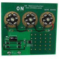
NUD4001 High Current LED Driver This device is designed to replace discrete solutions for driving LEDs in low voltage AC−DC applications 5 external resistor allows the circuit designer to set the drive current ...

Page 2

MAXIMUM RATINGS (T = 25°C unless otherwise noted) A Rating Continuous Input Voltage Non−repetitive Peak Input Voltage (t v 1.0 ms) Output Current (For V ≤ 2.2 V) (Note 1) drop Output Voltage Human Body Model (HBM) Maximum ratings are ...

Page 3

I (mA) OUT Figure 1. Output Current (I vs. External Resistor (R 1.200 1.000 0.800 0.600 0.400 0.200 0.000 AMBIENT TEMPERATURE (°C) A Figure 3. ...

Page 4

Design Guide 1. Define LED’s current 350 mA LED 2. Calculate Resistor Value for (see Figure ext sense 0 °C)/ 0.350 = 2.0 ...

Page 5

D1 1N4004 R1 2 bat 13.5 Vdc − 0 Figure 7. Stop light automotive circuit using the NUD4001 device D1 1N4004 R1 7 bat 13.5 Vdc − 0 Figure 8. ...

Page 6

V bat 12 Vdc − Figure 9. NUD4001 Device Configuration for PWM D1 MURA105T3 12 Vac from Transformer or Electronic Transformer D3 MURA105T3 Figure 10. 12 Vac landscape lighting application circuit using the NUD4001 device to drive ...

Page 7

NUD4001 Power Dissipation The power dissipation of the SO− function of the pad size. This can vary from the minimum pad size for soldering to a pad size given for maximum power dissipation. Power dissipation for a surface ...

Page 8

... *For additional information on our Pb−Free strategy and soldering details, please download the ON Semiconductor Soldering and Mounting Techniques Reference Manual, SOLDERRM/D. Thermal Clad is a registered trademark of the Bergquist Company. ON Semiconductor and are registered trademarks of Semiconductor Components Industries, LLC (SCILLC). SCILLC reserves the right to make changes without further notice to any products herein ...

Related keywords