NCP1421LEDEVB ON Semiconductor, NCP1421LEDEVB Datasheet - Page 2
NCP1421LEDEVB
Manufacturer Part Number
NCP1421LEDEVB
Description
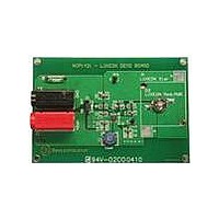
EVAL BOARD FOR NCP1421LED
Manufacturer
ON Semiconductor
Specifications of NCP1421LEDEVB
Design Resources
NCP1421LEDEVB BOM NCP1421LEDEVB Schematic NCP1421LEDEVB Gerber Files
Current - Output / Channel
600mA
Outputs And Type
1, Non-Isolated
Voltage - Output
500 ~ 700 mV
Voltage - Input
3.6V
Utilized Ic / Part
NCP1421
Core Chip
NCP1421
Topology
Boost
No. Of Outputs
1
Output Current
600mA
Development Tool Type
Hardware - Eval/Demo Board
Mcu Supported Families
NCP1421
Lead Free Status / RoHS Status
Lead free / RoHS Compliant
Features
-
Lead Free Status / Rohs Status
Lead free / RoHS Compliant
For Use With/related Products
NCP1421LED
Other names
NCP1421LEDEVBOS


Design Steps
components for this circuit. (R2, R3, R4, L1) This shows the
600 mA version as an example:
(Find value of V
equal dependence on V
reference and R4. One could increase the output voltage by
making the voltage across R4 (V
power dissipation in R4 by lowering V
must equal 1.2 V, and that is 0.6 V
to the above calculated value. Choose R2 = 475 kW.
one−cell Li−ion battery pack or a 3−cell NiMH pack so the
1000
The following steps show how to determine the critical
Step 1: Let LED current = I
Step 2: From the LED datasheet, let V
Step 3: Let R3 = 100 kW
Step 4: Let V
Step 5: For I
Step 6: Now, V
Step 7: So, R2 = (V
Step 8: Then choose a standard value of R2 which is close
Step 9: Pick input voltage range. These circuits assume a
(3.5/0.6) * 100 kW − 100 kW = 483 kW
900
800
700
600
500
400
300
200
100
0
3.0
Figure 2. Output Current vs. Input Voltage
3.2
D
R4
600 mA
200 mA
F
800 mA
= 600 mA and V
R4
at 600 mA).
= 0.5 * V
plus the divided voltage off of the LED
F
3.4
INPUT VOLTAGE (V)
/(V
F
ref
variation and tolerance of the
ref
− V
D
100
Figure 4. Electrical to Optical Efficiency vs. Input Voltage
3.6
95
90
85
80
75
70
65
60
55
50
which is 0.6 V. This places
= 600 mA
3.0
R4
R4
R4
)) * R3 − R3 =
200 mA
800 mA
600 mA
V
= 0.6 V, R4 = 1.0 W.
) larger or decrease
F
R4
= 3.5 V @ 600 mA
3.8
F
.
3.2
= 3.5 V
4.0
3.4
INPUT VOLTAGE (V)
http://onsemi.com
AND8171/D
4.2
3.6
2
V
input voltage is assumed to be 3.6 V and has been optimized
around this point.
V
because this circuit decreases LED current as V
from the designed value. This is shown by the following
equation: I
it increases current as V
but then the difference between V
peak current is reduced.
determine the appropriate L1, C1, and C2. For this
application, 6.8
over the load and line range.
this circuit V
(1−V
840 mA
inductor with an I
F
100
F
Step 10: Determine output voltage. Output voltage will be
Step 11: Use the NCP1421 or NCP1422 datasheet to
Step 12: Determine the inductor saturation current. For
Step 13: Add 20% margin to this I
95
90
85
80
75
70
65
60
55
50
= 3.5 V @ 600 mA
3.8
+ V
3.0
in
200 mA
600 mA
/V
Figure 3. Converter Efficiency vs. Input Voltage
R4
800 mA
out
= 4.1 V One can use the 3.6 V as V
D
4.0
). Therefore I
3.2
= 1/R4*(V
in
m
min = 3 V: I
H, 22
sat
4.2
> 1.0 A.
3.4
INPUT VOLTAGE (V)
m
F
ref
F, and 22
Lavg
decreases from the designed value,
− V
Lavg
= 600 mA/(1−(1−V
3.6
F
*(R3/R2 + R3)) Conversely
m
= I
F were found to work well
in
V
and V
out
F
= 3.5 V @ 600 mA
3.8
/ (1−D) where D =
Lavg
out
in
is less, so the
chosen above
and pick an
4.0
F
in
increases
/V
out
)) =
4.2
Related parts for NCP1421LEDEVB
Image
Part Number
Description
Manufacturer
Datasheet
Request
R

Part Number:
Description:
600 Ma Sync-rect Pfm Step-up Dc-dc Converter Step-up Dc-dc Converter With True-cutoff And Ring-killer
Manufacturer:
ON Semiconductor
Datasheet:

Part Number:
Description:
EVAL BOARD FOR NCP1421
Manufacturer:
ON Semiconductor
Datasheet:
Part Number:
Description:
ON Semiconductor [VOLTAGE REGULATOR]
Manufacturer:
ON Semiconductor
Datasheet:
Part Number:
Description:
357-036-542-201 CARDEDGE 36POS DL .156 BLK LOPRO
Manufacturer:
ON Semiconductor
Datasheet:
Part Number:
Description:
357-036-542-201 CARDEDGE 36POS DL .156 BLK LOPRO
Manufacturer:
ON Semiconductor
Datasheet:
Part Number:
Description:
357-036-542-201 CARDEDGE 36POS DL .156 BLK LOPRO
Manufacturer:
ON Semiconductor
Datasheet:
Part Number:
Description:
357-036-542-201 CARDEDGE 36POS DL .156 BLK LOPRO
Manufacturer:
ON Semiconductor
Datasheet:
Part Number:
Description:
357-036-542-201 CARDEDGE 36POS DL .156 BLK LOPRO
Manufacturer:
ON Semiconductor
Datasheet:
Part Number:
Description:
357-036-542-201 CARDEDGE 36POS DL .156 BLK LOPRO
Manufacturer:
ON Semiconductor
Datasheet:
Part Number:
Description:
357-036-542-201 CARDEDGE 36POS DL .156 BLK LOPRO
Manufacturer:
ON Semiconductor
Datasheet:
Part Number:
Description:
357-036-542-201 CARDEDGE 36POS DL .156 BLK LOPRO
Manufacturer:
ON Semiconductor
Datasheet:
Part Number:
Description:
357-036-542-201 CARDEDGE 36POS DL .156 BLK LOPRO
Manufacturer:
ON Semiconductor
Datasheet:
Part Number:
Description:
357-036-542-201 CARDEDGE 36POS DL .156 BLK LOPRO
Manufacturer:
ON Semiconductor
Datasheet:
Part Number:
Description:
Manufacturer:
ON Semiconductor
Datasheet: