NCP565V12EVB ON Semiconductor, NCP565V12EVB Datasheet - Page 3
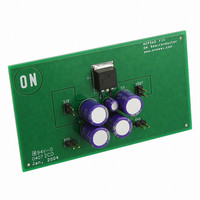
NCP565V12EVB
Manufacturer Part Number
NCP565V12EVB
Description
EVAL BOARD FOR NCP565V12
Manufacturer
ON Semiconductor
Specifications of NCP565V12EVB
Design Resources
NCP565 Demo Board BOM NCP565V12EVB Gerber Files NCP565 Fixed Demo Board Schematic
Channels Per Ic
1 - Single
Voltage - Output
1.2V
Current - Output
1.5A
Voltage - Input
4.5 ~ 5.5V
Regulator Type
Positive Fixed
Board Type
Fully Populated
Utilized Ic / Part
NCP565
Lead Free Status / RoHS Status
Lead free / RoHS Compliant
Operating Temperature
-
Lead Free Status / Rohs Status
Lead free / RoHS Compliant
For Use With/related Products
NCP565V12
Other names
NCP565V12EVBOS


Stresses exceeding Maximum Ratings may damage the device. Maximum Ratings are stress ratings only. Functional operation above the
Recommended Operating Conditions is not implied. Extended exposure to stresses above the Recommended Operating Conditions may affect
device reliability.
NOTE:
1. Refer to Electrical Characteristics and Application Information for Safe Operating Area.
2. As measured using a copper heat spreading area of 50 mm
3. Minimum V
ABSOLUTE MAXIMUM RATINGS
THERMAL CHARACTERISTICS
OPERATING RANGES
Input Voltage (Note 1)
Output Pin Voltage
Adjust Pin Voltage
Thermal Characteristics SOT−223 (Notes 1, 2)
Thermal Characteristics DFN6 (Notes 1, 2)
Thermal Characteristics D
Operating Input Voltage (Note 1)
Operating Junction Temperature Range
Operating Ambient Temperature Range
Storage Temperature Range
Thermal Resistance, Junction−to−Ambient
Thermal Resistance, Junction−to−Pin
Thermal Resistance, Junction−to−Ambient
Thermal Resistance, Junction−to−Pin
Thermal Resistance, Junction−to−Case
Thermal Resistance, Junction−to−Ambient
Thermal Resistance, Junction−to−Pin
This device series contains ESD protection and exceeds the following tests:
Human Body Model JESD 22−A114−B
Machine Model JESD 22−A115−A
in
= (V
out
+ V
2
DO
PAK (5ld) (Notes 1, 2)
) or 2.5 V, whichever is higher.
Rating
Rating
Rating
http://onsemi.com
2
, 1 oz copper thickness.
3
Symbol
Symbol
Symbol
R
R
R
R
R
R
R
V
V
T
V
V
T
T
out
adj
qJA
qJP
qJA
qJP
qJC
qJA
qJP
stg
in
in
A
J
2.5 (Note 3) to 9
−0.3 to V
−0.3 to V
V
−40 to 150
−40 to 125
−55 to 150
out
Value
Value
Value
107
176
105
+ V
18
12
37
3
4
in
in
DO
+ 0.3
+ 0.3
,
°C/W
°C/W
°C/W
Unit
Unit
Unit
°C
°C
°C
V
V
V
V
Related parts for NCP565V12EVB
Image
Part Number
Description
Manufacturer
Datasheet
Request
R

Part Number:
Description:
ON Semiconductor [VOLTAGE REGULATOR]
Manufacturer:
ON Semiconductor
Datasheet:
Part Number:
Description:
357-036-542-201 CARDEDGE 36POS DL .156 BLK LOPRO
Manufacturer:
ON Semiconductor
Datasheet:
Part Number:
Description:
357-036-542-201 CARDEDGE 36POS DL .156 BLK LOPRO
Manufacturer:
ON Semiconductor
Datasheet:
Part Number:
Description:
357-036-542-201 CARDEDGE 36POS DL .156 BLK LOPRO
Manufacturer:
ON Semiconductor
Datasheet:
Part Number:
Description:
357-036-542-201 CARDEDGE 36POS DL .156 BLK LOPRO
Manufacturer:
ON Semiconductor
Datasheet:
Part Number:
Description:
357-036-542-201 CARDEDGE 36POS DL .156 BLK LOPRO
Manufacturer:
ON Semiconductor
Datasheet:
Part Number:
Description:
357-036-542-201 CARDEDGE 36POS DL .156 BLK LOPRO
Manufacturer:
ON Semiconductor
Datasheet:
Part Number:
Description:
357-036-542-201 CARDEDGE 36POS DL .156 BLK LOPRO
Manufacturer:
ON Semiconductor
Datasheet:
Part Number:
Description:
357-036-542-201 CARDEDGE 36POS DL .156 BLK LOPRO
Manufacturer:
ON Semiconductor
Datasheet:
Part Number:
Description:
357-036-542-201 CARDEDGE 36POS DL .156 BLK LOPRO
Manufacturer:
ON Semiconductor
Datasheet:
Part Number:
Description:
357-036-542-201 CARDEDGE 36POS DL .156 BLK LOPRO
Manufacturer:
ON Semiconductor
Datasheet:
Part Number:
Description:
Manufacturer:
ON Semiconductor
Datasheet:
Part Number:
Description:
Manufacturer:
ON Semiconductor
Datasheet:
Part Number:
Description:
Manufacturer:
ON Semiconductor
Datasheet: