NCP565VADJEVB ON Semiconductor, NCP565VADJEVB Datasheet - Page 9
NCP565VADJEVB
Manufacturer Part Number
NCP565VADJEVB
Description
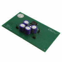
EVAL BOARD FOR NCP565VADJ
Manufacturer
ON Semiconductor
Specifications of NCP565VADJEVB
Design Resources
NCP565 ADJ Demo Board BOM NCP565VADJEVB Gerber Files NCP565 ADJ Demo Board Schematic
Channels Per Ic
1 - Single
Voltage - Output
3.3V
Current - Output
1.5A
Voltage - Input
5V
Regulator Type
Positive Fixed
Board Type
Fully Populated
Utilized Ic / Part
NCP565
Lead Free Status / RoHS Status
Lead free / RoHS Compliant
Operating Temperature
-
Lead Free Status / Rohs Status
Lead free / RoHS Compliant
For Use With/related Products
NCP565VADJ
Other names
NCP565VADJEVBOS


PCB Layout Considerations
good load transient performance. Because it is very sensitive
to its PCB layout, particular care has to be taken when
tackling Printed Circuit Board (PCB) layout. The figures
below give an example of a layout where parasitic elements
are minimized. For microprocessor applications it is
customary to use an output capacitor network consisting of
Good PCB layout plays an important role in achieving
GND
V
in
Figure 20. Schematic of NCP565 Typical Application Circuit
C
150 m
1
C
150 m
2
Figure 21. Top Layer
http://onsemi.com
2
1
NC
V
in
NCP565
GND
3
9
15.8 k
R
V
several capacitors in parallel. This reduces the overall ESR
and reduces the instantaneous output voltage drop under
transient load conditions. The output capacitor network
should be as close as possible to the load for the best results.
The schematic of NCP565 typical application circuit, which
this PCB layout is base on, is shown in Figure 20. The output
voltage is set to 3.3 V for this demonstration board according
to the feedback resistors in the Table 1.
Adj
out
2
4
5
5.6 p
42.2 k
C
R
6
C
10 m
1
4
C
150 m
3
GND
C
150 m
V
out
3
Related parts for NCP565VADJEVB
Image
Part Number
Description
Manufacturer
Datasheet
Request
R

Part Number:
Description:
ON Semiconductor [VOLTAGE REGULATOR]
Manufacturer:
ON Semiconductor
Datasheet:
Part Number:
Description:
357-036-542-201 CARDEDGE 36POS DL .156 BLK LOPRO
Manufacturer:
ON Semiconductor
Datasheet:
Part Number:
Description:
357-036-542-201 CARDEDGE 36POS DL .156 BLK LOPRO
Manufacturer:
ON Semiconductor
Datasheet:
Part Number:
Description:
357-036-542-201 CARDEDGE 36POS DL .156 BLK LOPRO
Manufacturer:
ON Semiconductor
Datasheet:
Part Number:
Description:
357-036-542-201 CARDEDGE 36POS DL .156 BLK LOPRO
Manufacturer:
ON Semiconductor
Datasheet:
Part Number:
Description:
357-036-542-201 CARDEDGE 36POS DL .156 BLK LOPRO
Manufacturer:
ON Semiconductor
Datasheet:
Part Number:
Description:
357-036-542-201 CARDEDGE 36POS DL .156 BLK LOPRO
Manufacturer:
ON Semiconductor
Datasheet:
Part Number:
Description:
357-036-542-201 CARDEDGE 36POS DL .156 BLK LOPRO
Manufacturer:
ON Semiconductor
Datasheet:
Part Number:
Description:
357-036-542-201 CARDEDGE 36POS DL .156 BLK LOPRO
Manufacturer:
ON Semiconductor
Datasheet:
Part Number:
Description:
357-036-542-201 CARDEDGE 36POS DL .156 BLK LOPRO
Manufacturer:
ON Semiconductor
Datasheet:
Part Number:
Description:
357-036-542-201 CARDEDGE 36POS DL .156 BLK LOPRO
Manufacturer:
ON Semiconductor
Datasheet:
Part Number:
Description:
Manufacturer:
ON Semiconductor
Datasheet:
Part Number:
Description:
Manufacturer:
ON Semiconductor
Datasheet:
Part Number:
Description:
Manufacturer:
ON Semiconductor
Datasheet: