LP38512MR-ADJEV/NOPB National Semiconductor, LP38512MR-ADJEV/NOPB Datasheet - Page 4
LP38512MR-ADJEV/NOPB
Manufacturer Part Number
LP38512MR-ADJEV/NOPB
Description
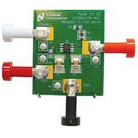
BOARD EVALUATION FOR LP38512
Manufacturer
National Semiconductor
Datasheets
1.LP38512MR-ADJEVNOPB.pdf
(14 pages)
2.LP38512MR-ADJEVNOPB.pdf
(8 pages)
3.LP38512MR-ADJEVNOPB.pdf
(14 pages)
Specifications of LP38512MR-ADJEV/NOPB
Channels Per Ic
1 - Single
Voltage - Output
1.2V
Current - Output
1.5A
Voltage - Input
2.25 ~ 5.5V
Regulator Type
Positive Adjustable
Operating Temperature
-40°C ~ 125°C
Board Type
Fully Populated
Utilized Ic / Part
LP38512
Silicon Manufacturer
National
Silicon Core Number
LP38512MR-ADJ
Kit Application Type
Power Management - Voltage Regulator
Application Sub Type
LDO
Kit Contents
Board, Doc
Lead Free Status / RoHS Status
Contains lead / RoHS non-compliant
Other names
LP38512MR-ADJEV


www.national.com
AC Parameters
Thermal Characteristics
Note 1: Absolute Maximum Ratings indicate limits beyond which damage to the device may occur. Operating Ratings indicate conditions for which the device is
intended to be functional, but does not guarantee specific performance limits. For guaranteed specifications and conditions, see the Electrical Characteristics.
Note 2: The human body model is a 100 pF capacitor discharged through a 1.5 kΩ resistor into each pin. Test method is per JESD22-A114.
Note 3: Refer to JEDEC J-STD-020C for surface mount device (SMD) package reflow profiles and conditions. Unless otherwise stated, the temperatures and
times are for Sn-Pb (STD) only.
Note 4: Device operation must be evaluated, and derated as needed, based on ambient temperature (T
junction temperature (T
(EIA/JESD51-3). See POWER DISSIPATION/HEAT-SINKING for details.
Note 5: Line regulation is defined as the change in V
Note 6: Load regulation is defined as the change in V
Note 7: The line and load regulation specification contains only the typical number. However, the limits for line and load regulation are included in the output
voltage tolerance specification.
Note 8: Dropout voltage (V
voltage to drop 2%. For the LP38512-ADJ, the minimum operating voltage of 2.25V is the limiting factor when the programed output voltage is less than typically
1.80V.
Symbol
PSRR
ΔT
ρ
T
θ
θ
e
n(l/f)
J-A
J-C
SD
n
SD
Ripple Rejection
Output Noise Density
Output Noise Voltage
Thermal Shutdown
Thermal Shutdown Hysteresis T
Thermal Resistance
Junction to Ambient
(Note 4)
Thermal Resistance
Junction to Case
J(MAX)
DO
), and package thermal resistance (θ
Parameter
) is typically defined as the input to output voltage differential (V
ADJ
ADJ
V
f = 120Hz
V
f = 1 kHz
f = 120Hz
BW = 10Hz - 100kHz
T
PSOP-8
TO-263 THIN
PSOP-8
TO-263 THIN
from the nominal value due to change in the voltage at the input.
from the nominal value due to change in the load current at the output.
IN
IN
J
J
rising
falling from T
= 2.5V
= 2.5V
JA
).The typical θ
Conditions
SD
4
JA
ratings given are worst case based on minimum land area on two-layer PCB
IN
- V
OUT
) where the input voltage is low enough to cause the output
A
), power dissipation (P
Min
-
-
-
-
-
-
-
-
-
-
Typ
165
168
0.4
73
70
25
10
67
11
3
D
), maximum allowable operating
Max
-
-
-
-
-
-
-
-
-
-
µV/
µV
Units
°C/W
°C/W
dB
°C
√
RMS
Hz
Related parts for LP38512MR-ADJEV/NOPB
Image
Part Number
Description
Manufacturer
Datasheet
Request
R

Part Number:
Description:
IC REG LDO 1.5A ADJ 8-PSOP
Manufacturer:
National Semiconductor
Datasheet:

Part Number:
Description:
National Semiconductor [8-Bit D/A Converter]
Manufacturer:
National Semiconductor
Datasheet:
Part Number:
Description:
National Semiconductor [Media Coprocessor]
Manufacturer:
National Semiconductor
Datasheet:
Part Number:
Description:
Digitally Controlled Tone and Volume Circuit with Stereo Audio Power Amplifier, Microphone Preamp Stage and National 3D Sound
Manufacturer:
National Semiconductor
Datasheet:
Part Number:
Description:
Digitally Controlled Tone and Volume Circuit with Stereo Audio Power Amplifier, Microphone Preamp Stage and National 3D Sound
Manufacturer:
National Semiconductor
Datasheet:
Part Number:
Description:
AC97 Rev 2 Codec with Sample Rate Conversion and National 3D Sound
Manufacturer:
National Semiconductor
Part Number:
Description:
Manufacturer:
National Semiconductor
Datasheet:
Part Number:
Description:
Manufacturer:
National Semiconductor
Datasheet:
Part Number:
Description:
General Purpose, Low Voltage, Low Power, Rail-to-Rail Output Operational Amplifiers
Manufacturer:
National Semiconductor
Datasheet:
Part Number:
Description:
8-bit 20 MSPS flash A/D converter.
Manufacturer:
National Semiconductor
Datasheet:
Part Number:
Description:
Low Noise Quad Operational Amplifier
Manufacturer:
National Semiconductor
Datasheet:
Part Number:
Description:
Quad Differential Line Receivers
Manufacturer:
National Semiconductor
Datasheet:
Part Number:
Description:
Quad High Speed Trapezoidal? Bus Transceiver
Manufacturer:
National Semiconductor
Datasheet:
Part Number:
Description:
Dual Line Receiver
Manufacturer:
National Semiconductor
Datasheet: