LMP8601MAEVAL/NOPB National Semiconductor, LMP8601MAEVAL/NOPB Datasheet - Page 2
LMP8601MAEVAL/NOPB
Manufacturer Part Number
LMP8601MAEVAL/NOPB
Description
BOARD EVALUATION FOR LMP8601MA
Manufacturer
National Semiconductor
Series
LMP®r
Specifications of LMP8601MAEVAL/NOPB
Channels Per Ic
1 - Single
Amplifier Type
Current Sense
Output Type
Single-Ended
Slew Rate
0.83 V/µs
Current - Output / Channel
48mA
Operating Temperature
-40°C ~ 125°C
Current - Supply (main Ic)
1.1mA
Voltage - Supply, Single/dual (±)
3 V ~ 5.5 V
Board Type
Fully Populated
Utilized Ic / Part
LMP8601
Silicon Manufacturer
National
Silicon Core Number
LMP8601, LMP8601Q
Kit Application Type
Amplifier
Application Sub Type
Current-Sense Amplifier
Kit Contents
Board, Doc
Lead Free Status / RoHS Status
Lead free / RoHS Compliant
-3db Bandwidth
-
Other names
LMP8601MAEVAL


www.national.com
Description of the LMP8601
Evaluation Board
The LMP8601 evaluation board requires a power supply with
a voltage between 3.0V and 5.5V , the supply current will be
<2 mA in normal operation with high impedance load on the
output of the part. The positive supply voltage is connected to
V
(P6).
The offset voltage on the output of the LMP8601 is deter-
mined by the voltage on the offset pin which is connected to
pin2 of J1 and the offset voltage will be V
normally connected with a jumper to GND or V
can also be driven from a low impedance source (<10 Ω).
With a jumper on J1 between 1–2 the offset pin is connected
to V
configuration the LMP8601 can be used for measuring bidi-
rectional currents.
PCB Layout Guidelines
This section provides general practical guidelines for PCB
layouts that use various power and ground traces. Designers
should note that these are only "rule-of-thumb" recommen-
dations and the actual results are predicated on the final
layout.
DIFFERENTIAL SIGNALS
The two input pins of the LMP8601 form a differential pair that
must be handled following the rules given below.
•
S
Keep both signals coupled by routing them closely
together and keeping them of equal length.
(P5) The negative supply voltage is connected to GND
S
and the offset voltage is half the value of V
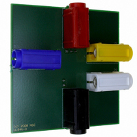
FIGURE 2. Power Supply Connectors and Headers
Offset
/2. This pin is
S
, but this pin
S
. In this
2
With a jumper on J1 between 2–3 the offset pin is connected
to GND and the output voltage is ground referenced. In this
configuration the LMP8601 is used for measuring unidirec-
tional currents.
The input signal is connected between +IN (P1) and −IN (P2)
and the output signal is available at OUT (P3).
On the board there is the possibility to place a capacitor C2
which creates a low pass filter between the first and second
stage. This can be used to reduce the output noise and glitch-
es that might appear from switching large common mode
voltages with very fast transients at the input . (Please see the
application section of the LMP8601 data sheet for more de-
tails about this filter).
the Header J2 is normally shorted with a jumper and connects
the first stage to the second stage . The application section of
the LMP8601 data sheet explains more about the alternative
configurations that can be made after removing the jumper on
J2.
•
•
POWER, GROUND AND DE-COUPLING
Keep the power supply de-coupling capacitor close to the
power supply pin (V
Make sure all return currents of the signals can flow next to
the originating signals
Do not allow any other signal in between these two signals
of the differential pair.
Keep all impedances in both traces of the signal equal.
S
of the part.)
30089704
Related parts for LMP8601MAEVAL/NOPB
Image
Part Number
Description
Manufacturer
Datasheet
Request
R

Part Number:
Description:
National Semiconductor [8-Bit D/A Converter]
Manufacturer:
National Semiconductor
Datasheet:
Part Number:
Description:
National Semiconductor [Media Coprocessor]
Manufacturer:
National Semiconductor
Datasheet:
Part Number:
Description:
Digitally Controlled Tone and Volume Circuit with Stereo Audio Power Amplifier, Microphone Preamp Stage and National 3D Sound
Manufacturer:
National Semiconductor
Datasheet:
Part Number:
Description:
Digitally Controlled Tone and Volume Circuit with Stereo Audio Power Amplifier, Microphone Preamp Stage and National 3D Sound
Manufacturer:
National Semiconductor
Datasheet:
Part Number:
Description:
AC97 Rev 2 Codec with Sample Rate Conversion and National 3D Sound
Manufacturer:
National Semiconductor
Part Number:
Description:
Manufacturer:
National Semiconductor
Datasheet:
Part Number:
Description:
Manufacturer:
National Semiconductor
Datasheet:
Part Number:
Description:
General Purpose, Low Voltage, Low Power, Rail-to-Rail Output Operational Amplifiers
Manufacturer:
National Semiconductor
Datasheet:
Part Number:
Description:
8-bit 20 MSPS flash A/D converter.
Manufacturer:
National Semiconductor
Datasheet:
Part Number:
Description:
Low Noise Quad Operational Amplifier
Manufacturer:
National Semiconductor
Datasheet:
Part Number:
Description:
Quad Differential Line Receivers
Manufacturer:
National Semiconductor
Datasheet:
Part Number:
Description:
Quad High Speed Trapezoidal? Bus Transceiver
Manufacturer:
National Semiconductor
Datasheet:
Part Number:
Description:
Dual Line Receiver
Manufacturer:
National Semiconductor
Datasheet:
Part Number:
Description:
TTL to 10k ECL Level Translator with Latch
Manufacturer:
National Semiconductor
Datasheet: