TMPSNS-RTD1 Microchip Technology, TMPSNS-RTD1 Datasheet - Page 3
TMPSNS-RTD1
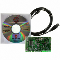
Manufacturer Part Number
TMPSNS-RTD1
Description
BOARD EVAL PT100 RTD TEMP SENSOR
Manufacturer
Microchip Technology
Datasheets
1.MCP3301-CIMS.pdf
(32 pages)
2.PCM18XR1.pdf
(438 pages)
3.MCP6S22DM-PICTL.pdf
(43 pages)
4.TMPSNS-RTD1.pdf
(26 pages)
Specifications of TMPSNS-RTD1
Sensor Type
Temperature
Interface
USB
Embedded
Yes, MCU, 8-Bit
Utilized Ic / Part
MCP3301, MCP6S26, PIC18F2550
Processor To Be Evaluated
MCP6S26, MCP3301, MCP6024, MCP41010, PIC18F2550, TC1071, MCP6002
Data Bus Width
12 bit
Interface Type
USB
Lead Free Status / RoHS Status
Not applicable / Not applicable
Voltage - Supply
-
Sensitivity
-
Sensing Range
-
Lead Free Status / RoHS Status
Lead free / RoHS Compliant, Not applicable / Not applicable


1.0
Maximum Ratings*
V
All inputs and outputs w.r.t. V
Storage temperature .......................... -65°C to +150°C
Ambient temp. with power applied ..... -65°C to +125°C
Maximum Junction Temperature ....................... 150°C
ESD protection on all pins (HBM)......................... > 4 kV
*Notice: Stresses above those listed under “Maximum rat-
ings” may cause permanent damage to the device. This is a
stress rating only and functional operation of the device at
those or any other conditions above those indicated in the
operational listings of this specification is not implied. Expo-
sure to maximum rating conditions for extended periods may
affect device reliability.
ELECTRICAL SPECIFICATIONS
© 2007 Microchip Technology Inc.
Electrical Characteristics: Unless otherwise noted, all parameters apply at V
configuration (Figure 3-4) with fixed common mode voltage of 2.5V. All parameters apply over temperature with
T
Conversion Rate
Maximum Sampling Frequency
Conversion Time
Acquisition Time
DC Accuracy
Resolution
Integral Nonlinearity
Differential Nonlinearity
Positive Gain Error
Negative Gain Error
Offset Error
Dynamic Performance
Total Harmonic Distortion
Signal to Noise and Distortion
Spurious Free Dynamic Range
Common-Mode Rejection
Power Supply Rejection
Note 1: This specification is established by characterization and not 100% tested.
DD
AMB
........................................................................ 7.0V
= -40°C to +85°C (Note 7). Conversion speed (f
2: See characterization graphs that relate converter performance to V
3: V
4: V
5: Maximum clock frequency specification must be met.
6: V
7: MSOP devices are only specified at 25°C and +85°C.
8: For slow sample rates, see Section 6.2.1 for limitations on clock frequency.
ELECTRICAL
CHARACTERISTICS
IN
DD
REF
Parameter
= 0.1V to 4.9V @ 1 kHz.
= 5VDC ±500 mV
= 400 mV, V
IN
= 0.1V to 4.9V @ 1 kHz
SS
P
.......-0.3V to V
-
P
@ 1 kHz, see test circuit Figure 3-3.
Symbol
f
SAMPLE
SINAD
CMRR
SFDR
t
PSR
CONV
t
DNL
THD
INL
ACQ
DD
SAMPLE)
+0.3V
Min
—
—
—
—
—
—
—
—
—
-3
-3
-3
—
12 data bits + sign
is 100 ksps with f
-0.75
±0.5
±0.5
Typ
-0.5
-91
±1
+3
78
92
79
74
—
—
1.5
13
PIN FUNCTION TABLE
V
IN(+)
IN(-)
V
CS/SHDN
D
CLK
V
REF
SS
DD
OUT
Name
Max
100
50
±1
±2
±1
+2
+2
+6
—
—
—
—
—
DD
REF
CLK
= 5V, V
level.
= 17*f
periods
periods
Reference Voltage Input
Positive Analog Input
Negative Analog Input
Ground
Chip Select / Shutdown Input
Serial Data Out
Serial Clock
+2.7V to 5.5V Power Supply
Units
ksps
ksps
CLK
CLK
LSB
LSB
LSB
LSB
LSB
SS
bits
SAMPLE
dB
dB
dB
dB
dB
= 0V, and V
Note 8
V
MCP3301-B
MCP3301-C
Monotonic with no missing codes
over temperature
Note 3
Note 3
Note 3
Note 6
Note 4
DD
= V
REF
Function
REF
MCP3301
= 5V. Full differential input
Conditions
= 2.7V, V
DS21700C-page 3
CM
=1.35V
Related parts for TMPSNS-RTD1
Image
Part Number
Description
Manufacturer
Datasheet
Request
R

Part Number:
Description:
Manufacturer:
Microchip Technology Inc.
Datasheet:
Part Number:
Description:
Manufacturer:
Microchip Technology Inc.
Datasheet:
Part Number:
Description:
Manufacturer:
Microchip Technology Inc.
Datasheet:
Part Number:
Description:
Manufacturer:
Microchip Technology Inc.
Datasheet:
Part Number:
Description:
Manufacturer:
Microchip Technology Inc.
Datasheet:
Part Number:
Description:
Manufacturer:
Microchip Technology Inc.
Datasheet:
Part Number:
Description:
Manufacturer:
Microchip Technology Inc.
Datasheet:
Part Number:
Description:
Manufacturer:
Microchip Technology Inc.
Datasheet: