EVALB1127 Fujitsu Semiconductor America Inc, EVALB1127 Datasheet - Page 9
EVALB1127
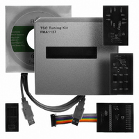
Manufacturer Part Number
EVALB1127
Description
KIT TUNING/DEV BOARD
Manufacturer
Fujitsu Semiconductor America Inc
Specifications of EVALB1127
Sensor Type
Touch, Capacitive
Interface
I²C
Voltage - Supply
2.3 V ~ 5.5 V
Embedded
No
Utilized Ic / Part
FMA1127
Lead Free Status / RoHS Status
Lead free / RoHS Compliant
Sensitivity
-
Sensing Range
-
Other names
865-1051


Communication Specifications for I
Table 1: DC Electrical Specifications for I
Note:
1. Devices that use non-standard supply voltages which do not conform to the intended I
2. Maximum V
3. C
4. The maximum t
5. I/O pins of Fast-mode devices must not obstruct the SDA and SCL lines if V
6. VIH=1.21V, VIL=0.76V. Hence hysteresis is about 0.45V at the condition of 500KHz input frequency. Input impedance Cin is about 2pF.
n/a = not applicable
the pull-up resistors R
series protection resistors (R
specified for t
b
Symbol
= capacitance of one bus line in pF.
V
V
V
V
V
Iol
t
t
OL1
OL3
C
hys
sp
I
of
IH
IL
i
i
IH
f
.
= V
f
for the SDA and SCL bus lines quoted in Table 2 (300ns) is longer than the specified maximum t
LOW Level Input Voltage:
HIGH Level Input Voltage:
Hysteresis of Schmitt Trigger Inputs:
LOW Level Output Voltage (open drain or collector)
at 3mA Sink Current:
Digital Output Low Current at
Output Fall Time from V
Capacitance from 10pF to 400pF
Pulse Width of Spike Which Must be Suppressed by
the Input Filter
Input Current each I/O Pin with an Input Voltage
Between 0.1V
Capacitance for Each I/O Pin
DDmax
Fixed Input Levels
V
Fixed Input Levels
V
V
V
V
V
Vol = 0.6V
Vol = 0.4V
p
DD
DD
DD
DD
DD
DD
are connected.
+ 0.5V.
Related Input Levels
Related Input Levels
> 2V
< 2V
> 2V
< 2V
S
) to be connected between the SDA/SCL pins and the SDA/SCL bus lines as shown in Figure 6 without exceeding the maximum
DD
and 0.9V V
Parameter
IHmin
DDmax
to V
ILmax
2
C Bus
with a Bus
DD
0.7 x V
0.7 x V
is switched off.
Min.
-0.5
-0.5
-10
3.0
3.0
n/a
n/a
0
Standard-Mode
2
DD
DD
2
C
C bus system levels must relate their input levels to the V
0.3 V
250
Max.
1.5
0.4
n/a
8.4
5.7
n/a
10
10
(2)
(2)
(2)
(2)
(4)
DD
20 + 0.1Cb
of
0.7 x V
0.7 x V
for the output stages (250ns). The allows
-10
Min.
-0.5
n/a
n/a
n/a
0
0
0
(5)
DD
DD
Fast-Mode
(3)
FMA1127DC
Fujitsu Microelectronics America, Inc.
0.3 x V
0.2 x V
10
Max
n/a
n/a
n/a
0.4
8.4
5.7
50
10
(2)
(2)
(5)
DD (1)
DD
DD
voltage to which
Unit
mA
mA
μA
ns
ns
pF
V
V
V
V
V
V
V
V
7
Related parts for EVALB1127
Image
Part Number
Description
Manufacturer
Datasheet
Request
R

Part Number:
Description:
IC POWER SUPPLY MONITOR 8SOP
Manufacturer:
Fujitsu Semiconductor America Inc
Datasheet:
Part Number:
Description:
IC POWER SUPPLY MONITOR 8SOP
Manufacturer:
Fujitsu Semiconductor America Inc
Datasheet:

Part Number:
Description:
IC MCU 60K FLASH 2KB RAM 52LQFP
Manufacturer:
Fujitsu Semiconductor America Inc
Datasheet:

Part Number:
Description:
IC MCU 32BIT 256KB FLASH 120LQFP
Manufacturer:
Fujitsu Semiconductor America Inc
Datasheet:
Part Number:
Description:
IC CTLR TOUCH SENSOR 12CH 30SSOP
Manufacturer:
Fujitsu Semiconductor America Inc
Datasheet:

Part Number:
Description:
IC CTLR TOUCH SENSOR 12CH 40QFN
Manufacturer:
Fujitsu Semiconductor America Inc
Datasheet:
Part Number:
Description:
SYNTHESIZER PLL DUAL INP 20SSOP
Manufacturer:
Fujitsu Semiconductor America Inc
Datasheet:

Part Number:
Description:
SYNTHESZR PLL 1.1GHZ DUAL 16SSOP
Manufacturer:
Fujitsu Semiconductor America Inc
Datasheet:

Part Number:
Description:
IC SSCG EMI RED 8-SOIC
Manufacturer:
Fujitsu Semiconductor America Inc
Datasheet:

Part Number:
Description:
IC SSCG EMI RED 8-TSSOP
Manufacturer:
Fujitsu Semiconductor America Inc
Datasheet:

Part Number:
Description:
IC SSCG EMI RED 8-SOP
Manufacturer:
Fujitsu Semiconductor America Inc
Datasheet:

Part Number:
Description:
SYNTHESIZER PLL 2.5GHZ 16SSOP
Manufacturer:
Fujitsu Semiconductor America Inc
Datasheet:
Part Number:
Description:
SYNTHESIZER PLL 1.2GHZ 16SSOP
Manufacturer:
Fujitsu Semiconductor America Inc
Datasheet:

Part Number:
Description:
SYNTHESIZER PLL 2.5GHZ 16BCC
Manufacturer:
Fujitsu Semiconductor America Inc
Datasheet:

Part Number:
Description:
IC SSCG EMI RED 8-SOP
Manufacturer:
Fujitsu Semiconductor America Inc
Datasheet: