STEVAL-MKI031V1 STMicroelectronics, STEVAL-MKI031V1 Datasheet - Page 21

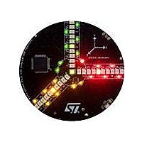
STEVAL-MKI031V1
Manufacturer Part Number
STEVAL-MKI031V1
Description
PLATFORM MUSA
Manufacturer
STMicroelectronics
Datasheets
1.STEVAL-MKI009V1.pdf
(42 pages)
2.STEVAL-MKI022V1.pdf
(38 pages)
3.STEVAL-MKI031V1.pdf
(9 pages)
4.STEVAL-MKI094V1.pdf
(34 pages)
Specifications of STEVAL-MKI031V1
Sensor Type
*
Sensing Range
*
Interface
*
Sensitivity
*
Embedded
Yes, MCU, 8-Bit
Utilized Ic / Part
*
Voltage - Supply
*
Sensing Axis
Double Axis
Output Type
Digital
Interface Type
USB
Lead Free Status / RoHS Status
Lead free / RoHS Compliant
For Use With/related Products
LPR5xxxAL, LPY5xxxAL, LY5xxxAL
Other names
497-10672
LIS331DLH
5.2.2
The SPI Read command is performed with 16 clock pulses. Multiple byte read command is
performed adding blocks of 8 clock pulses at the previous one.
bit 0: READ bit. The value is 1.
bit 1: MS bit. When 0 do not increment address, when 1 increment address in multiple
reading.
bit 2-7: address AD(5:0). This is the address field of the indexed register.
bit 8-15: data DO(7:0) (read mode). This is the data that will be read from the device (MSb
first).
bit 16-... : data DO(...-8). Further data in multiple byte reading.
Figure 8.
SPI write
Figure 9.
The SPI Write command is performed with 16 clock pulses. Multiple byte write command is
performed adding blocks of 8 clock pulses at the previous one.
bit 0: WRITE bit. The value is 0.
bit 1: MS bit. When 0 do not increment address, when 1 increment address in multiple
writing.
bit 2 -7: address AD(5:0). This is the address field of the indexed register.
bit 8-15: data DI(7:0) (write mode). This is the data that is written inside the device (MSb
first).
bit 16-... : data DI(...-8). Further data in multiple byte writing.
SDO
SPC
SDI
CS
SPC
SDI
CS
Multiple bytes SPI read protocol (2 bytes example)
SPI write protocol
RW
MS
AD5 AD4 AD3 AD2 AD1 AD0
RW
MS
AD5 AD4 AD3 AD2 AD1 AD0
Doc ID 15094 Rev 3
DO7 DO6 DO5 DO4 DO3 DO2 DO1 DO0
DI7 DI6 DI5 DI4 DI3 DI2 DI1 DI0
DO15 DO14 DO13 DO12 DO11 DO10 DO9 DO8
Digital interfaces
21/38


