SI85XX-EVB Silicon Laboratories Inc, SI85XX-EVB Datasheet - Page 13
SI85XX-EVB
Manufacturer Part Number
SI85XX-EVB
Description
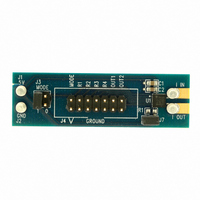
BOARD EVAL CURRENT SENSOR 10A
Manufacturer
Silicon Laboratories Inc
Datasheet
1.SI85XX-EVB.pdf
(36 pages)
Specifications of SI85XX-EVB
Sensor Type
Current Sensor
Sensing Range
10A
Interface
Analog
Voltage - Supply
2.7 V ~ 5.5 V
Embedded
No
Utilized Ic / Part
Si8512
Lead Free Status / RoHS Status
Lead free / RoHS Compliant
Sensitivity
-
Lead Free Status / Rohs Status
Supplier Unconfirmed
Other names
336-1425
Available stocks
Company
Part Number
Manufacturer
Quantity
Price
Company:

Part Number:
SI85XX-EVB
Manufacturer:
Silicon Laboratories Inc
Quantity:
135


3. Application Information
3.1. Board Layout
The Si85xx is connected in the series path of the current
to be measured. The Si85xx must be located as far as
possible from transformer and other magnetic field
sources. Like other analog components, the Si85xx
should be powered from a low-noise dc source and,
preferably, to a low-noise analog ground plane.
Recommended bypass capacitors are 1 µF in parallel
with a 0.1 µF, positioned as close to the Si85xx as
possible. When using the Si850x (single output
versions), all 3 ground pins MUST be connected to the
same ground point, and both VDD and VDD2 pins
MUST be tied to VDD.
3.2. SOIC Layout Requirements
The Si85xx SOIC package version requires special
layout techniques to ensure proper operation. Due to
the large SOIC package seize and close proximity of the
current-carrying slug and current sensor silicon,
magnetic coupling between the current-carrying slug
and the silicon can form a ground loop causing the
output voltage to be 0 V even though current is flowing
through the slug. To eliminate any such coupling issues,
a red fly-wire VDD trace as shown in Figure 9 should be
implemented in the layout for the SOIC package. The
red fly-wire trace should be approximately 3.5 mm from
the
approximately in the center of the package. Standard
wire thicknesses for 10 mA current-carrying capabilities
should be used. Note also that any ground planes
should be moved to the edge of the package.
center
edge
of
the
package
intersecting
Preliminary Rev. 0.21
Regarding isolation voltage requirements, the trace
does not need to follow the lead frame and bonding
traces exactly, as long as the net magnetic flux is close
to zero. The goal here is to keep the magnetic coupling
small and, at the same time, keep the isolation distance
large. Moreover, to ensure that the layout meets the
design’s
requirements, the VDD trace should be placed on one
of the inner layers or even the back side of the board.
For example, one can lay out the return VDD trace on
the other side of the PCB so the PCB itself can help to
provide high isolation voltage.
PCB VDD Trace
Bonding wire
cut here
5V VDD trace
(non-ping-pong)
Gnd pin
Figure 9. SOIC Layout Requirements
VDD fly wire
Mode pin
VDD pin
plane edge
Ground
required
3.5 mm
creepage
SOIC package
Top View
and
Si85xx
clearance
carrying slug
sensor die
plane edge
Current
Ground
Current
13
Related parts for SI85XX-EVB
Image
Part Number
Description
Manufacturer
Datasheet
Request
R

Part Number:
Description:
SMT Power Inductor
Manufacturer:
ETC
Datasheet:
Part Number:
Description:
Smt Power Inductor
Manufacturer:
ETC-unknow
Datasheet:
Part Number:
Description:
Power Inductor
Manufacturer:
ETC-unknow
Datasheet:
Part Number:
Description:
SMT Power Inductor
Manufacturer:
ETC [List of Unclassifed Manufacturers]
Datasheet:

Part Number:
Description:
SMD/C°/SINGLE-ENDED OUTPUT SILICON OSCILLATOR
Manufacturer:
Silicon Laboratories Inc
Part Number:
Description:
Manufacturer:
Silicon Laboratories Inc
Datasheet:
Part Number:
Description:
N/A N/A/SI4010 AES KEYFOB DEMO WITH LCD RX
Manufacturer:
Silicon Laboratories Inc
Datasheet:
Part Number:
Description:
N/A N/A/SI4010 SIMPLIFIED KEY FOB DEMO WITH LED RX
Manufacturer:
Silicon Laboratories Inc
Datasheet:
Part Number:
Description:
N/A/-40 TO 85 OC/EZLINK MODULE; F930/4432 HIGH BAND (REV E/B1)
Manufacturer:
Silicon Laboratories Inc
Part Number:
Description:
EZLink Module; F930/4432 Low Band (rev e/B1)
Manufacturer:
Silicon Laboratories Inc
Part Number:
Description:
I°/4460 10 DBM RADIO TEST CARD 434 MHZ
Manufacturer:
Silicon Laboratories Inc
Part Number:
Description:
I°/4461 14 DBM RADIO TEST CARD 868 MHZ
Manufacturer:
Silicon Laboratories Inc
Part Number:
Description:
I°/4463 20 DBM RFSWITCH RADIO TEST CARD 460 MHZ
Manufacturer:
Silicon Laboratories Inc