AT91SAM9260-EK Atmel, AT91SAM9260-EK Datasheet - Page 21
AT91SAM9260-EK
Manufacturer Part Number
AT91SAM9260-EK
Description
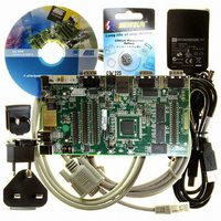
KIT EVAL FOR AT91SAM9260
Manufacturer
Atmel
Series
AT91SAM Smart ARMr
Type
MCUr
Datasheets
1.AT91SAM9260-EK.pdf
(47 pages)
2.AT91SAM9260-EK.pdf
(39 pages)
3.AT91SAM9260-EK.pdf
(10 pages)
Specifications of AT91SAM9260-EK
Contents
Evaluation Board, Parallel Cable and CD-ROM
Processor To Be Evaluated
AT91SAM9260
Data Bus Width
32 bit
Interface Type
RS-232, Ethernet, USB
Core
ARM 9
Silicon Manufacturer
Atmel
Core Architecture
ARM
Core Sub-architecture
ARM926EJ-S
Silicon Core Number
AT91SAM9260
Silicon Family Name
ARM
Kit Contents
Board, Cables, CD, Power Supply
Rohs Compliant
Yes
For Use With/related Products
AT91SAM9260
Lead Free Status / RoHS Status
Lead free / RoHS Compliant


8.1
8.1.1
6221JS–ATARM–17-Jul-09
Embedded Memories
Boot Strategies
A first level of address decoding is performed by the Bus Matrix, i.e., the implementation of the
Advanced High Performance Bus (AHB) for its Master and Slave interfaces with additional
features.
Decoding breaks up the 4G bytes of address space into 16 banks of 256 Mbytes. The banks 1 to
7 are directed to the EBI that associates these banks to the external chip selects EBI_NCS0 to
EBI_NCS7. Bank 0 is reserved for the addressing of the internal memories, and a second level
of decoding provides 1 Mbyte of internal memory area. Bank 15 is reserved for the peripherals
and provides access to the Advanced Peripheral Bus (APB).
Other areas are unused and performing an access within them provides an abort to the master
requesting such an access.
Each Master has its own bus and its own decoder, thus allowing a different memory mapping
per Master. However, in order to simplify the mappings, all the masters have a similar address
decoding.
Regarding Master 0 and Master 1 (ARM926 Instruction and Data), three different Slaves are
assigned to the memory space decoded at address 0x0: one for internal boot, one for external
boot, one after remap. Refer to
A complete memory map is presented in
Table 8-1
status and the BMS state at reset.
Table 8-1.
The system always boots at address 0x0. To ensure a maximum number of possibilities for boot,
the memory layout can be configured with two parameters.
REMAP allows the user to lay out the first internal SRAM bank to 0x0 to ease development. This
is done by software once the system has booted. Refer to the Bus Matrix Section for more
details.
When REMAP = 0, BMS allows the user to lay out to 0x0, at his convenience, the ROM or an
external memory. This is done via hardware at reset.
Note:
0x0000 0000
• 32 KB ROM
• Two 4 KB Fast SRAM
– Single Cycle Access at full matrix speed
– Single Cycle Access at full matrix speed
Memory blocks not affected by these parameters can always be seen at their specified base
addresses. See the complete memory map presented in
summarizes the Internal Memory Mapping for each Master, depending on the Remap
Address
Internal Memory Mapping
Table 8-1, “Internal Memory Mapping,” on page 21
REMAP = 0
BMS = 1
ROM
Figure 8-1 on page
BMS = 0
EBI_NCS0
Figure 8-1 on page 20
20.
AT91SAM9260
REMAP = 1
SRAM0 4K
.
for details.
21
Related parts for AT91SAM9260-EK
Image
Part Number
Description
Manufacturer
Datasheet
Request
R

Part Number:
Description:
MCU, MPU & DSP Development Tools KICKSTART KIT FOR AT91SAM9 PLUS
Manufacturer:
IAR Systems

Part Number:
Description:
DEV KIT FOR AVR/AVR32
Manufacturer:
Atmel
Datasheet:

Part Number:
Description:
INTERVAL AND WIPE/WASH WIPER CONTROL IC WITH DELAY
Manufacturer:
ATMEL Corporation
Datasheet:
Part Number:
Description:
Low-Voltage Voice-Switched IC for Hands-Free Operation
Manufacturer:
ATMEL Corporation
Datasheet:
Part Number:
Description:
MONOLITHIC INTEGRATED FEATUREPHONE CIRCUIT
Manufacturer:
ATMEL Corporation
Datasheet:
Part Number:
Description:
AM-FM Receiver IC U4255BM-M
Manufacturer:
ATMEL Corporation
Datasheet:
Part Number:
Description:
Monolithic Integrated Feature Phone Circuit
Manufacturer:
ATMEL Corporation
Datasheet:
Part Number:
Description:
Multistandard Video-IF and Quasi Parallel Sound Processing
Manufacturer:
ATMEL Corporation
Datasheet:
Part Number:
Description:
High-performance EE PLD
Manufacturer:
ATMEL Corporation
Datasheet:
Part Number:
Description:
8-bit Flash Microcontroller
Manufacturer:
ATMEL Corporation
Datasheet:
Part Number:
Description:
2-Wire Serial EEPROM
Manufacturer:
ATMEL Corporation
Datasheet: