DK-DEV-3SL150N Altera, DK-DEV-3SL150N Datasheet - Page 21
DK-DEV-3SL150N
Manufacturer Part Number
DK-DEV-3SL150N
Description
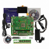
KIT DEVELOPMENT STRATIX III
Manufacturer
Altera
Series
Stratix® IIIr
Type
FPGAr
Datasheets
1.EP3SL150F780C4N.pdf
(16 pages)
2.EP3SL150F780C4N.pdf
(332 pages)
3.DK-DEV-3SL150N.pdf
(34 pages)
Specifications of DK-DEV-3SL150N
Contents
Development Platform, Cables and Software
Silicon Manufacturer
Altera
Core Architecture
FPGA
Core Sub-architecture
Stratix
Silicon Core Number
EP3S
Silicon Family Name
Stratix III
Kit Contents
Development Board, Cable And Accessories
Rohs Compliant
Yes
For Use With/related Products
EP3SL150F152
Lead Free Status / RoHS Status
Lead free / RoHS Compliant
Other names
544-2568
Available stocks
Company
Part Number
Manufacturer
Quantity
Price
Company:

Part Number:
DK-DEV-3SL150N
Manufacturer:
Altera
Quantity:
135


Chapter 5: Power Measurement
Measuring Power
Measuring Power
A/D Measurements
© August 2008 Altera Corporation
You can measure power by using the analog-to-digital (A/D) circuitry on the
development board or by using a digital multimeter (DMM) across on-board sense
resistors. However, note that, depending on the DMM accuracy, the on-board A/D
measurements tend to produce considerably more accurate results.
The POWER SELECT rotary switch SW6 sets the development board to measure and
display FPGA core power or I/O output power
Table 5–4. Switch SW6 Power Selection
Measuring Core Power
To measure FPGA core power for various power states, perform the following steps:
1. Ensure that the 8-position SW2 DIP switch is configured to the default settings
2. Download the stratixIII_dev_power.sof file as described in
3. Set the POWER SELECT rotary switch SW6 to 0 to measure the internal V
4. Observe the power on the 4-digit hexadecimal POWER DISPLAY.
5. Using the user input push buttons
Measuring I/O Power
This example uses FPGA I/O banks 2, 4, 5, and 6. Using the SW6 settings
measure the power for I/O banks 4, 5, and 6, then for I/O bank 2, by performing the
following steps:
1. Ensure that the 8-position SW2 DIP switch is configured to the default settings
2. Download the stratixIII_dev_power.sof file as described in
3. Set the POWER SELECT rotary switch SW6 to 8.
4. Observe the 4-digit hexadecimal POWER DISPLAY for the I/O output power in
shown in
FPGA” on page
<path>\demos\stratixIII_3sl150_dev_power.
power in watts.
power states in
as frequency and resources increase.
shown in
FPGA” on page
<path>\demos\stratixIII_3sl150_dev_power.
watts on banks 4, 5, and 6.
Switch Position
0
7
8
Table 4–1 on page
Table 4–1 on page
Table 5–2
4–3. The power design example is in
4–3. The power design example is in
Core: VCCL, TBD V
I/O: 2.5 V
I/O: 2.5 V
FPGA Power
and
4–2.
4–2.
Table 5–3 on page
(Table 5–1 on page
(Table
4, 5, and 6
5–2. Notice how power increases
I/O Bank
5–4).
—
2
5–1), advance through the
Stratix III Development Kit User Guide
“Configuring the
“Configuring the
(Table
CC_INT
5–4),
5–3
Related parts for DK-DEV-3SL150N
Image
Part Number
Description
Manufacturer
Datasheet
Request
R

Part Number:
Description:
KIT DEV ARRIA II GX FPGA 2AGX125
Manufacturer:
Altera
Datasheet:

Part Number:
Description:
KIT DEV CYCLONE III LS EP3CLS200
Manufacturer:
Altera
Datasheet:

Part Number:
Description:
KIT DEV STRATIX IV FPGA 4SE530
Manufacturer:
Altera
Datasheet:

Part Number:
Description:
KIT DEV FPGA 2AGX260 W/6.375G TX
Manufacturer:
Altera
Datasheet:

Part Number:
Description:
KIT DEV MAX V 5M570Z
Manufacturer:
Altera
Datasheet:

Part Number:
Description:
KIT DEV STRATIX V FPGA 5SGXEA7
Manufacturer:
Altera
Datasheet:

Part Number:
Description:
KIT DEVELOPMENT STRATIX IV
Manufacturer:
Altera
Datasheet:

Part Number:
Description:
KIT DEV ARRIA GX 1AGX60N
Manufacturer:
Altera
Datasheet:
Part Number:
Description:
KIT STARTER CYCLONE IV GX
Manufacturer:
Altera
Datasheet:
Part Number:
Description:
KIT DEVELOPMENT STRATIX IV
Manufacturer:
Altera
Datasheet:

Part Number:
Description:
CPLD, EP610 Family, ECMOS Process, 300 Gates, 16 Macro Cells, 16 Reg., 16 User I/Os, 5V Supply, 35 Speed Grade, 24DIP
Manufacturer:
Altera Corporation
Datasheet:
Part Number:
Description:
CPLD, EP610 Family, ECMOS Process, 300 Gates, 16 Macro Cells, 16 Reg., 16 User I/Os, 5V Supply, 15 Speed Grade, 24DIP
Manufacturer:
Altera Corporation
Datasheet: