DEMO908GZ60E Freescale Semiconductor, DEMO908GZ60E Datasheet - Page 11
DEMO908GZ60E
Manufacturer Part Number
DEMO908GZ60E
Description
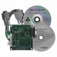
BOARD DEMO FOR 908GZ60 MCU
Manufacturer
Freescale Semiconductor
Series
HC08GRr
Type
MCUr
Specifications of DEMO908GZ60E
Design Resources
DEMO908GZ60E Schematic
Contents
Board, Cable, CD
Processor To Be Evaluated
908GZ
Data Bus Width
16 bit
Interface Type
RS-232
For Use With/related Products
68HC908GZ60
Lead Free Status / RoHS Status
Lead free / RoHS Compliant


D E M O 9 0 8 R G 6 0
A U G U S T
6 ,
2 0 0 4
Power Switch
A Power Switch (PWR_SW) has been provided between the input Terminal Block and the volt-
age regulator to allow the user to turn the board on and off. The Power Switch connects or
disconnects only power applied to the terminal block. Voltage applied to connector J1 is not
affected by this switch.
Reset Switch
The RESET switch provides a method to apply an asynchronous reset to the module. Press-
ing the RESET switch applies a low voltage level to the RST* input. A resistor tied to the high
voltage rail prevents spurious RESET input to the MCU. A capacitor tied to ground holds the
signal line low for a sufficient amount of time.
Timing
An 8 MHz ceramic resonator at Y1 provides timing to the DEMO908GZ60. This allows a de-
fault 4.0 MHz internal operating frequency. Using the embedded PLL, the internal bus fre-
quency can be increased to a maximum of 8 MHz. The resonator output is routed to the MCU
only and is not available at connector (J1).
Connectors J1 and J2
Connectors J1 and J2 are 40-pin, surface-mount, socket headers mounted on the bottom of
the module. Each connector is mounted over plated-through holes in the PCB. The socket is
a pass-through type socket designed to allow header insertion from either the top or bottom.
These connectors provide maximum flexibility allowing the module to connect directly to an ex-
panded development environment or to test equipment. Access to all MCU signals is available
at connector J1 or J2.
Power may be supplied to the module through pins J1-1 (+V) and J1-3 (GND). Use of this op-
tion requires input voltage between +4.75VDC and +5.25VDC. This input directly connects to
the module power and ground planes. Care should be exercised not to over-drive this input.
J1 can also be used to source power from the on-board regulator to external modules. The
PWR_SEL option header determines how power is routed to and from the module.
NOTE: Power output from the module is limited by the 250 mA maximum output of the on-board
voltage regulator.
The table below shows the pin-out for the MCU IO Connectors.
11
Related parts for DEMO908GZ60E
Image
Part Number
Description
Manufacturer
Datasheet
Request
R

Part Number:
Description:
Manufacturer:
Freescale Semiconductor, Inc
Datasheet:
Part Number:
Description:
Manufacturer:
Freescale Semiconductor, Inc
Datasheet:
Part Number:
Description:
Manufacturer:
Freescale Semiconductor, Inc
Datasheet:
Part Number:
Description:
Manufacturer:
Freescale Semiconductor, Inc
Datasheet:
Part Number:
Description:
Manufacturer:
Freescale Semiconductor, Inc
Datasheet:
Part Number:
Description:
Manufacturer:
Freescale Semiconductor, Inc
Datasheet:
Part Number:
Description:
Manufacturer:
Freescale Semiconductor, Inc
Datasheet:
Part Number:
Description:
Manufacturer:
Freescale Semiconductor, Inc
Datasheet:
Part Number:
Description:
Manufacturer:
Freescale Semiconductor, Inc
Datasheet:
Part Number:
Description:
Manufacturer:
Freescale Semiconductor, Inc
Datasheet:
Part Number:
Description:
Manufacturer:
Freescale Semiconductor, Inc
Datasheet:
Part Number:
Description:
Manufacturer:
Freescale Semiconductor, Inc
Datasheet:
Part Number:
Description:
Manufacturer:
Freescale Semiconductor, Inc
Datasheet:
Part Number:
Description:
Manufacturer:
Freescale Semiconductor, Inc
Datasheet:
Part Number:
Description:
Manufacturer:
Freescale Semiconductor, Inc
Datasheet: