C8051T630DK Silicon Laboratories Inc, C8051T630DK Datasheet - Page 11
C8051T630DK
Manufacturer Part Number
C8051T630DK
Description
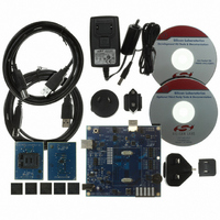
KIT DEV FOR C8051T630 FAMILY
Manufacturer
Silicon Laboratories Inc
Type
MCUr
Specifications of C8051T630DK
Contents
Board, daughter boards, power adapter, cables, documentation and software
Processor To Be Evaluated
C8051T63x
Interface Type
USB
Lead Free Status / RoHS Status
Lead free / RoHS Compliant
For Use With/related Products
C8051T630, T631, T632, T633, T634 and T635 MCUs
For Use With
336-1465 - BOARD SOCKET DAUGHTER 20-QFN
Lead Free Status / Rohs Status
Lead free / RoHS Compliant
Other names
336-1464


7.1. System Clock Sources
The C8051T63x devices feature a calibrated internal oscillator that is enabled as the system clock source on reset.
After reset, the internal oscillator operates at a frequency of 24.5 MHz (±2%) by default, but may be configured by
software to operate at other frequencies. Therefore, in many applications, an external oscillator is not required.
However, if you wish to operate the C8051T63x device at a frequency not available with the internal oscillator, an
external oscillator source may be used. Refer to the C8051T63x data sheet for more information on configuring the
system clock source.
7.2. Switches, LEDs, Potentiometer, and IDAC Resistor
Two switches are provided on the motherboard. The RESET switch is connected to the RST pin of the C8051T63x.
Pressing RESET puts the device into its hardware-reset state. The switch labeled “SW” can be connected to the
C8051T63x's general purpose I/O (GPIO) pin P0.7 through header J9. Pressing this switch generates a logic low
signal on the port pin. Remove the shorting block from the J9 header to disconnect the switch from the port pin.
Six LEDs are also provided on the motherboard. The red LED labeled “PWR” (D4), is used to indicate a power
connection to the motherboard. The green LED labeled “RUN” (D10) turns on when the debug circuitry is in a
running state; the red LED labeled “STOP” (D11) turns on when the debug circuitry is in a halted state, and the
orange LED labeled “DEBUG PWR” (D12) indicates whether the debug adapter circuit is being powered through
P5's USB connector. The red LED labeled “VPP” (D7) indicates when the VPP programming voltage is being
applied to the device. The green LED, labeled "LED" (D1), can be connected to the C8051T63x's GPIO pin through
header J9. Remove the shorting block from the header to disconnect the LED from the port pin. The red LED
labeled "USB ACTIVE" (D2) will turn on whenever the CP2103 USB-to-UART bridge is connected to a PC and has
successfully completed enumeration.
Also included on the C8051T63x motherboard is a 10 kΩ thumbwheel rotary potentiometer, reference number R8.
The potentiometer can be connected to the C8051T63x's P1.6 pin through the J12 header. Remove the shorting
block from the header to disconnect the potentiometer from the port pin.
A 1 kΩ resistor, reference number R20, is included on the C8051T63x Motherboard to provide a current path to
ground for the IDAC. The resistor can be connected to the IDAC output pin (P0.1) through the J5 header.
Table 1 lists the port pins and headers corresponding to the switches, LEDs, potentiometer, and IDAC resistor.
Orange LED labeled "DEBUG PWR"
Green LED labeled "USB ACTIVE"
Green LED labeled "RUN"
Green LED labeled "LED"
Red LED labeled "STOP"
Red LED labeled "PWR"
Red LED labeled “VPP”
IDAC Resistor
Potentiometer
Description
RESET
SW
Table 1. Motherboard I/O Descriptions
Component Name
SW1
SW2
D10
D12
R20
D11
D1
D2
D4
D7
R8
Rev. 0.1
Daughter Card's RST/C2CK
U2 CP2103's SUSPEND
Debug Adapter Signal
Debug Adapter Signal
Debug Adapter Signal
Daughter Card's P0.7
Daughter Card's P1.3
Daughter Card's VDD
Daughter Card's P0.2
Daughter Card's P1.6
Daughter Card's P0.1
I/O
C8051T63x-DK
Header
J9 [3-4]
J9 [1-2]
J6, J7
None
None
None
None
None
J12
J11
J5
11
Related parts for C8051T630DK
Image
Part Number
Description
Manufacturer
Datasheet
Request
R

Part Number:
Description:
SMD/C°/SINGLE-ENDED OUTPUT SILICON OSCILLATOR
Manufacturer:
Silicon Laboratories Inc
Part Number:
Description:
Manufacturer:
Silicon Laboratories Inc
Datasheet:
Part Number:
Description:
N/A N/A/SI4010 AES KEYFOB DEMO WITH LCD RX
Manufacturer:
Silicon Laboratories Inc
Datasheet:
Part Number:
Description:
N/A N/A/SI4010 SIMPLIFIED KEY FOB DEMO WITH LED RX
Manufacturer:
Silicon Laboratories Inc
Datasheet:
Part Number:
Description:
N/A/-40 TO 85 OC/EZLINK MODULE; F930/4432 HIGH BAND (REV E/B1)
Manufacturer:
Silicon Laboratories Inc
Part Number:
Description:
EZLink Module; F930/4432 Low Band (rev e/B1)
Manufacturer:
Silicon Laboratories Inc
Part Number:
Description:
I°/4460 10 DBM RADIO TEST CARD 434 MHZ
Manufacturer:
Silicon Laboratories Inc
Part Number:
Description:
I°/4461 14 DBM RADIO TEST CARD 868 MHZ
Manufacturer:
Silicon Laboratories Inc
Part Number:
Description:
I°/4463 20 DBM RFSWITCH RADIO TEST CARD 460 MHZ
Manufacturer:
Silicon Laboratories Inc
Part Number:
Description:
I°/4463 20 DBM RADIO TEST CARD 868 MHZ
Manufacturer:
Silicon Laboratories Inc
Part Number:
Description:
I°/4463 27 DBM RADIO TEST CARD 868 MHZ
Manufacturer:
Silicon Laboratories Inc
Part Number:
Description:
I°/4463 SKYWORKS 30 DBM RADIO TEST CARD 915 MHZ
Manufacturer:
Silicon Laboratories Inc
Part Number:
Description:
N/A N/A/-40 TO 85 OC/4463 RFMD 30 DBM RADIO TEST CARD 915 MHZ
Manufacturer:
Silicon Laboratories Inc
Part Number:
Description:
I°/4463 20 DBM RADIO TEST CARD 169 MHZ
Manufacturer:
Silicon Laboratories Inc