M52223EVB Freescale Semiconductor, M52223EVB Datasheet - Page 38
M52223EVB
Manufacturer Part Number
M52223EVB
Description
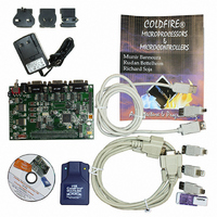
BOARD EVAL FOR MCF52223
Manufacturer
Freescale Semiconductor
Series
ColdFire®r
Type
MPUr
Datasheet
1.M52221DEMO.pdf
(56 pages)
Specifications of M52223EVB
Contents
SBC, Cables and Software
Processor To Be Evaluated
MCF5222x
Interface Type
RS-232
Silicon Manufacturer
Freescale
Core Architecture
Coldfire
Core Sub-architecture
Coldfire V2
Silicon Core Number
MCF52
Silicon Family Name
MCF5222x
Rohs Compliant
Yes
For Use With/related Products
MCF52223
Lead Free Status / RoHS Status
Lead free / RoHS Compliant


Electrical Characteristics
2.12
Figure 10-17 shows the ADC input circuit during sample and hold. S1 and S2 are always open/closed at the same time that S3
is closed/open. When S1/S2 are closed & S3 is open, one input of the sample and hold circuit moves to (V
the other charges to the analog input voltage. When the switches are flipped, the charge on C1 and C2 are averaged via S3, with
the result that a single-ended analog input is switched to a differential voltage centered about (V
switch on every cycle of the ADC clock (open one-half ADC clock, closed one-half ADC clock). There are additional
capacitances associated with the analog input pad, routing, etc., but these do not filter into the S/H output voltage, as S1 provides
isolation during the charge-sharing phase. One aspect of this circuit is that there is an on-going input current, which is a function
of the analog input voltage, V
38
1
2
3
4
5
6
7
All measurements are made at V
INL measured from V
LSB = Least Significant Bit
INL measured from V
Includes power-up of ADC and V
ADC clock cycles
Current that can be injected or sourced from an unselected ADC signal input without impacting the performance of the ADC
SINAD
ENOB
Name
SFDR
THD
1.
2.
3.
4.
5.
Parasitic capacitance due to package, pin-to-pin and pin-to-package base coupling; 1.8pF
Parasitic capacitance due to the chip bond pad, ESD protection devices and signal routing; 2.04pF
Equivalent resistance for the channel select mux; 100 Ωs
Sampling capacitor at the sample and hold circuit. Capacitor C1 is normally disconnected from the input and is only
connected to it at sampling time; 1.4pF
Equivalent input impedance, when the input is selected =
Analog Input
Equivalent Circuit for ADC Inputs
Total harmonic distortion
Spurious free dynamic range
Signal-to-noise plus distortion
Effective number of bits
1
IN
IN
= V
= 0.1V
REF
REFL
2
REFH
Characteristic
and the ADC clock frequency.
to V
REF
DD
Figure 9. Equivalent Circuit for A/D Loading
to V
= 3.3V, V
IN
Table 32. ADC Parameters
MCF52223 ColdFire Microcontroller, Rev. 2
= V
IN
REFH
= 0.9V
125W ESD Resistor
REFH
REFH
(V
= 3.3V, and V
REFH
3
- V
REFL
)/ 2
REFL
(ADC Clock Rate) × (1.4×10
8pF noise damping capacitor
S1
1
= ground
(continued)
S2
Min
9.1
—
—
—
1
4
S3
67 to 70.3
61 to 63.9
Typical
10.6
−75
C2
C1
-12
)
REFH
S/H
Freescale Semiconductor
-V
C1 = C2 = 1pF
Max
REFL
REFH
—
—
—
—
)/2. The switches
-V
REFL
)/2, while
Unit
Bits
dB
dB
dB
Related parts for M52223EVB
Image
Part Number
Description
Manufacturer
Datasheet
Request
R

Part Number:
Description:
Manufacturer:
Freescale Semiconductor, Inc
Datasheet:
Part Number:
Description:
Manufacturer:
Freescale Semiconductor, Inc
Datasheet:
Part Number:
Description:
Manufacturer:
Freescale Semiconductor, Inc
Datasheet:
Part Number:
Description:
Manufacturer:
Freescale Semiconductor, Inc
Datasheet:
Part Number:
Description:
Manufacturer:
Freescale Semiconductor, Inc
Datasheet:
Part Number:
Description:
Manufacturer:
Freescale Semiconductor, Inc
Datasheet:
Part Number:
Description:
Manufacturer:
Freescale Semiconductor, Inc
Datasheet:
Part Number:
Description:
Manufacturer:
Freescale Semiconductor, Inc
Datasheet:
Part Number:
Description:
Manufacturer:
Freescale Semiconductor, Inc
Datasheet:
Part Number:
Description:
Manufacturer:
Freescale Semiconductor, Inc
Datasheet:
Part Number:
Description:
Manufacturer:
Freescale Semiconductor, Inc
Datasheet:
Part Number:
Description:
Manufacturer:
Freescale Semiconductor, Inc
Datasheet:
Part Number:
Description:
Manufacturer:
Freescale Semiconductor, Inc
Datasheet:
Part Number:
Description:
Manufacturer:
Freescale Semiconductor, Inc
Datasheet:
Part Number:
Description:
Manufacturer:
Freescale Semiconductor, Inc
Datasheet: