C8051F540-TB Silicon Laboratories Inc, C8051F540-TB Datasheet
C8051F540-TB
Specifications of C8051F540-TB


Related parts for C8051F540-TB

C8051F540-TB Summary of contents
Page 1
... MCU family. The members of this MCU family are: C8051F540, C8051F541, C8051F542, C8051F543, C8051F544, C8051F545, C8051F546, and C8051F547. The target board included in this kit is provided with a pre-soldered C8051F540 MCU (QFN32 package) and a C8051F542 (QFN24 package). Code developed on the C8051F540 can be easily ported to the other members of this MCU family. ...
Page 2
... To install the IDE, utilities, and code examples, perform the following steps: 1. Click on the "Install Development Tools" button on the installation utility's startup screen the Kit Selection box that appears, choose the C8051F540DK development kit from the list of options the next screen, choose “Components to be Installed”. The programs necessary to download and debug on the MCU are the Silicon Labs IDE and the Keil 8051 Evaluation Toolset ...
Page 3
... To complete the installation process, connect the included USB cable between the host computer and the USB connector (P5) on the C8051F540 Target Board. Windows will automatically finish the driver installation. Information windows will pop up from the taskbar to show the installation progress. ...
Page 4
... C8051F540DK 5.1.2. Getting Started With the Silicon Labs IDE The following sections discuss how to open an example project in the IDE, build the source code, and download it to the target device. 5.1.2.1. Running the F540_Blinky example program The F540_Blinky example program blinks an LED on the target board. ...
Page 5
... For more information, please refer to the uVision driver documentation. The documentation and software are available from the Downloads webpage (www.silabs.com/mcudownloads). C8051F540DK Rev. 0.1 5 ...
Page 6
... Port I/O crossbar, configuring a timer for an interrupt routine, initializing the system clock, and configuring a GPIO port pin. When compiled/assembled and linked, this program flashes the green LED on the C8051F540 Target Board about five times a second using the interrupt handler with a C8051F540 timer. ...
Page 7
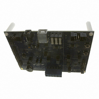
... Target Board The C8051F540 Development Kit includes a target board with a C8051F540 (Side A) and C8051F542 (Side B) device pre-installed for evaluation and preliminary software development. Numerous input/output (I/O) connections are provided to facilitate prototyping using the target board. Refer to Figure 3 for the locations of the various I/O connectors ...
Page 8
... RESET_A SIDE “A” Port 2 “A” P1.3_A 1 2 DS2 J3 P1.4_A Port 1 “A” J16 J15 Port 0 “A” J17 SILICON LABS J1 C8051F540- R22 Figure 3. C8051F540 Target Board with Pin Numbers TB1 P5 J18 CP P4 2102 COMM DS1 U1 J13 C8051 J14 F540 ...
Page 9
... J18 RESET_A SIDE “A” Port 2 “A” P1.3_A DS2 J3 P1.4_A Port 1 “A” J16 J2 J15 Port 0 “A” J17 SILICON LABS J1 www.silabs.com C8051F540-TB R22 Figure 4. C8051F540 Target Board Shorting Blocks: Factory Defaults P1 TB1 2102 COMM DS1 U1 J13 C8051 J14 F540 J8 ...
Page 10
... Target Board Power Options and Current Measurement (J4, J8, J24, P1, TB1) The MCUs on the C8051F540 Target Board are powered from net. The +5 V net is connected to the headers J8 (Side A) and J4 (Side B). Shorting blocks can be put on each header to connect the +5 V net to the VREGIN and VIO pins on the two MCUs ...
Page 11
... Two push-button switches are provided on the target board for each MCU. Switch RESET_A is connected to the RST pin of the C8051F540. Switch RESET_B is connected to the RST pin of the C8051F542. Pressing RESET_A puts the C8051F540 device into its hardware-reset state, and similarly for RESET_B and the C8051F542 MCU. ...
Page 12
... UART0 of the C8051F540 (Side A). The Silicon Labs CP2102 USB-to-UART bridge provides data connectivity between the C8051F540 and the PC via a USB port. The TX and RX signals of UART0 may be connected to the CP2102 by installing shorting blocks on header J14. The shorting block positions for connecting each of these signals to the CP2102 are listed in Table 3. To use this interface, the USB-to-UART device drivers should be installed as described in Section 4.3. " ...
Page 13
... Port I/O Connectors (J1-J3 and J5-J7) Each of the parallel ports of the C8051F540 (Side A) and C8051F542 (Side B) has its own 10-pin header connector. Each connector provides a pin for the corresponding port pins 0– VIO, and digital ground. The same pin-out is used for all of the port connectors. ...
Page 14
... C8051F540DK 7.11. Power Supply I/O (Side A) (TB3) All of the C8051F540 target device’s supply pins are connected to the TB3 terminal block. Refer to Table 8 for the TB3 terminal block connections. Table 8. TB3 Terminal Block Pin Descriptions 7.12. Alternate Power Supply Headers (J15, J18) The C8051F540 Target Board includes two headers that allow for alternate power sources and power measurement ...
Page 15
... Some GPIO pins of the C8051F540 MCU can have an alternate fixed function. For example, pin 30 on the C8051F540 MCU is designated P0.4, and can be used as a GPIO pin. Also, if the UART0 peripheral on the MCU is enabled using the crossbar registers, the TX signal is routed to this pin. This is shown in the "Alternate Fixed Function" ...
Page 16
... C8051F540DK Table 9. C8051F540 Target Board Pin Assignments and Headers (Continued) MCU Pin Name Pin# Primary Function P3.0 9 RST/C2CK 12 VIO 2 VREGIN 3 VREGIN VDD 4 VDDA 5 GND 6 GNDA 7 *Note: Headers denoted by this symbol are not directly connected to the MCU pin; the connection might be via one or more headers and/or pin-sharing resistor(s) ...
Page 17
... Schematics C8051F540DK Rev. 0.1 17 ...
Page 18
... C8051F540DK 18 Rev. 0.1 ...
Page 19
... C8051F540DK Rev. 0.1 19 ...
Page 20
... C8051F540DK 20 Rev. 0.1 ...
Page 21
... N : OTES C8051F540DK Rev. 0.1 21 ...
Page 22
... C8051F540DK C I ONTACT NFORMATION Silicon Laboratories Inc. 400 West Cesar Chavez Austin, TX 78701 Tel: 1+(512) 416-8500 Fax: 1+(512) 416-9669 Toll Free: 1+(877) 444-3032 Please visit the Silicon Labs Technical Support web page: https://www.silabs.com/support/pages/contacttechnicalsupport.aspx and register to submit a technical support request. The information in this document is believed to be accurate in all respects at the time of publication but is subject to change without notice. ...