DEMO9RS08LA8 Freescale Semiconductor, DEMO9RS08LA8 Datasheet - Page 8
DEMO9RS08LA8
Manufacturer Part Number
DEMO9RS08LA8
Description
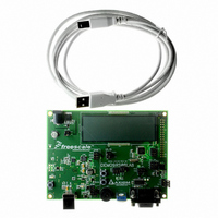
BOARD DEMO FOR MC9RSOLA8 MCU
Manufacturer
Freescale Semiconductor
Series
RS08r
Type
MCUr
Datasheets
1.DEMO9RS08LA8.pdf
(14 pages)
2.DEMO9RS08LA8.pdf
(8 pages)
3.DEMO9RS08LA8.pdf
(34 pages)
4.DEMO9RS08LA8.pdf
(2 pages)
Specifications of DEMO9RS08LA8
Contents
Board, Cable, DVD
Silicon Manufacturer
Freescale
Core Architecture
RS08
Core Sub-architecture
RS08
Silicon Core Number
MC9RS08
Silicon Family Name
RS08LA
Kit Contents
Board Cables CD Docs
Rohs Compliant
Yes
For Use With/related Products
MC9RS08LA8
Lead Free Status / RoHS Status
Contains lead / RoHS non-compliant
Available stocks
Company
Part Number
Manufacturer
Quantity
Price
Company:

Part Number:
DEMO9RS08LA8
Manufacturer:
Freescale Semiconductor
Quantity:
135


D E M O 9 R S 0 8 L A 8
U S E R
Figure 2: JP401 Option Header
BDM_PORT Header
A compatible HCS12 BDM cable can also attach to the 6-pin BDM interface header
(BDM_PORT). This header is not installed in default configuration. The figure below shows
the pin-out for the DEBUG header. This information is included for completeness.
Figure 3: J301 Header
POWER
The DEMO9RSO8LA8 provides several methods to apply power to the board. An option
header allows selection between the various power inputs. For application development and
debug, the board may be powered from the USB BDM. The 2.0mm PWR connector supports
stand-alone operation and higher power requirements. Power may also be applied to
connector J1 or the board may be configured to supply power from connector J1 to external
circuitry.
POWER SELECT
Power may be applied to the board through the integrated USB-Multilink BDM circuitry, a
2.0mm barrel connector, or through connector J1.
selection headers: the V_SEL option header and the VX_EN option header.
G U I D E
NOTE: This header is not installed in default configuration.
NOTE: On Rev A prototypes, J301-4 has been disconnected. To use an external BDM cable,
install a 6-pin header at J310 then add a wire from J301-4 to C400 (+).
BKGD
• • DATA1
• • DATA2
• • RXD
• • TXD
Damage to the board may result if voltage greater than +5.5V is applied to
1
3
5
2
4
6
GND
RESET*
VDD
Timer channel 0 input to Signal Analyzer
Timer channel 1 input to Signal Analyzer
SCI RXD input to Virtual COM Port
SCI TXD input to Virtual COM Port
the connector J1 input.
See the MC9RSO8LA8 Data Sheet for complete
DEBUG documentation
CAUTION:
8
Power selection is achieved using 2
J A N U A R Y
2 3 ,
2 0 0 8
Related parts for DEMO9RS08LA8
Image
Part Number
Description
Manufacturer
Datasheet
Request
R

Part Number:
Description:
Manufacturer:
Freescale Semiconductor, Inc
Datasheet:
Part Number:
Description:
Manufacturer:
Freescale Semiconductor, Inc
Datasheet:
Part Number:
Description:
Manufacturer:
Freescale Semiconductor, Inc
Datasheet:
Part Number:
Description:
Manufacturer:
Freescale Semiconductor, Inc
Datasheet:
Part Number:
Description:
Manufacturer:
Freescale Semiconductor, Inc
Datasheet:
Part Number:
Description:
Manufacturer:
Freescale Semiconductor, Inc
Datasheet:
Part Number:
Description:
Manufacturer:
Freescale Semiconductor, Inc
Datasheet:
Part Number:
Description:
Manufacturer:
Freescale Semiconductor, Inc
Datasheet:
Part Number:
Description:
Manufacturer:
Freescale Semiconductor, Inc
Datasheet:
Part Number:
Description:
Manufacturer:
Freescale Semiconductor, Inc
Datasheet:
Part Number:
Description:
Manufacturer:
Freescale Semiconductor, Inc
Datasheet:
Part Number:
Description:
Manufacturer:
Freescale Semiconductor, Inc
Datasheet:
Part Number:
Description:
Manufacturer:
Freescale Semiconductor, Inc
Datasheet:
Part Number:
Description:
Manufacturer:
Freescale Semiconductor, Inc
Datasheet:
Part Number:
Description:
Manufacturer:
Freescale Semiconductor, Inc
Datasheet: