DEMO9S12NE64E Freescale Semiconductor, DEMO9S12NE64E Datasheet - Page 16
DEMO9S12NE64E
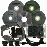
Manufacturer Part Number
DEMO9S12NE64E
Description
DEMO BOARD FOR 9S12NE64
Manufacturer
Freescale Semiconductor
Type
MCUr
Datasheet
1.DEMO9S12NE64E.pdf
(21 pages)
Specifications of DEMO9S12NE64E
Contents
*
Processor To Be Evaluated
MC9S12NE64
Maximum Operating Temperature
+ 50 C
Minimum Operating Temperature
- 10 C
Operating Supply Voltage
6 V to 12 V
Silicon Manufacturer
Freescale
Core Architecture
S12
Core Sub-architecture
S12
Silicon Core Number
MC9S12
Silicon Family Name
S12NE
Rohs Compliant
Yes
For Use With/related Products
MC9S12NE64
Lead Free Status / RoHS Status
Lead free / RoHS Compliant


2.4 SCI Connector J53
Freescale Semiconductor
1, 4, 6
7, 8, 9
Pin
2
3
5
DCD_B, DTR_B,
DSR_B
Label
RXD
GND
TXD
NC
Connector J53 is the SCI connector which is pinned out according to the DCE
format. Figure 2-2 and Table 2-3 give pin assignments and signal descriptions
for connector J53.
Table 2-3 SCI Connector J53 Signal Descriptions
DEMO9S12NE64 User’s Manual, Rev. 0.8
Pins 1, 4 and 6 are the active-low Data Carrier Detect, Data Terminal Ready,
and Data Set Ready signals. These pins are connected together through zero
ohm resistors. To disconnect pin 1 from pin 4, remove R58. To disconnect pin
6 from pin 4, remove R57
Pin 2 is the transmit data pin. It is connected to PS<1> of the MC9S12NE64
through a MAX3243 RS-232 Line Driver
Pin 3 is the receive data pin. It is connected to PS<0> of the MC9S12NE64
through a MAX3243 RS-232 Line Driver
GROUND
Pins 7, 8 , and 9 can be used as active-low Request to Send (RTS_B), Clear to
Send (CTS_B), and Ring Indicator (RI_B) pins. These pins on J53 are not
connected on the DEMO9S12NE64. If these pins need to be utilized, they can
be accessed through the unpopulated one pin headers J28, J27, and J26
respectively
Figure 2-2 SCI Connector J53 Pin Assignments
5
6
4
7
3
Signal
8
2
9
1
Support Information
19
Related parts for DEMO9S12NE64E
Image
Part Number
Description
Manufacturer
Datasheet
Request
R

Part Number:
Description:
Manufacturer:
Freescale Semiconductor, Inc
Datasheet:
Part Number:
Description:
Manufacturer:
Freescale Semiconductor, Inc
Datasheet:
Part Number:
Description:
Manufacturer:
Freescale Semiconductor, Inc
Datasheet:
Part Number:
Description:
Manufacturer:
Freescale Semiconductor, Inc
Datasheet:
Part Number:
Description:
Manufacturer:
Freescale Semiconductor, Inc
Datasheet:
Part Number:
Description:
Manufacturer:
Freescale Semiconductor, Inc
Datasheet:
Part Number:
Description:
Manufacturer:
Freescale Semiconductor, Inc
Datasheet:
Part Number:
Description:
Manufacturer:
Freescale Semiconductor, Inc
Datasheet:
Part Number:
Description:
Manufacturer:
Freescale Semiconductor, Inc
Datasheet:
Part Number:
Description:
Manufacturer:
Freescale Semiconductor, Inc
Datasheet:
Part Number:
Description:
Manufacturer:
Freescale Semiconductor, Inc
Datasheet:
Part Number:
Description:
Manufacturer:
Freescale Semiconductor, Inc
Datasheet:
Part Number:
Description:
Manufacturer:
Freescale Semiconductor, Inc
Datasheet:
Part Number:
Description:
Manufacturer:
Freescale Semiconductor, Inc
Datasheet:
Part Number:
Description:
Manufacturer:
Freescale Semiconductor, Inc
Datasheet: