M54455EVB Freescale Semiconductor, M54455EVB Datasheet
M54455EVB
Specifications of M54455EVB


Related parts for M54455EVB

M54455EVB Summary of contents
Page 1
... MC34702 Switch-Mode with Linear Power Supply Datasheet © Freescale Semiconductor, Inc., 2008. All rights reserved. 1 Introduction . . . . . . . . . . . . . . . . . . . . . . . . . . . . . . . . . . . 1 2 Overview . . . . . . . . . . . . . . . . . . . . . . . . . . . . . . . . . . . . . 2 2.1 MCF54455 Overview 2.2 M54455EVB Overview . . . . . . . . . . . . . . . . . . . . . . 4 2.3 Memory Map Overview . . . . . . . . . . . . . . . . . . . . . . 6 2.4 I/O Back Panel . . . . . . . . . . . . . . . . . . . . . . . . . . . . 7 3 Installation and Configuration . . . . . . . . . . . . . . . . . . . . . 7 4 Hardware Submodules . . . . . . . . . . . . . . . . . . . . . . . . . . 8 4.1 DDR SDRAM Interface . . . . . . . . . . . . . . . . . . . . . . 9 4 ...
Page 2
... DDR2 SDRAM Specification (JESD79-2C) 2 Overview 2.1 MCF54455 Overview The MCF54455 is the host processor for the M54455EVB. the MCF54455 superset device. The following is a brief summary of the functional blocks in the MCF54455 superset device. • Version 4 ColdFire Core with MMU and EMAC — 410 Dhrystone 2.1 MIPS @ 266 MHz • ...
Page 3
... RNG – Random Number Generator RTC – Real time clock SSI – Synchronous Serial Interface USB OTG – Universal Serial Bus On-the-Go controller Figure 1. MCF54455 Block Diagram M54455EVB User’s Manual, Rev. 4 Oscillator PLL 2 FECs USB OTG PCI Serial Boot SDRAM ...
Page 4
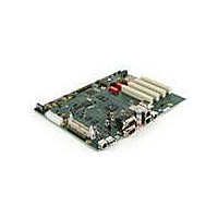
... M54455EVB Overview The M54455EVB provides hardware to evaluate as many of the configurations of the MCF5445x family as possible. The M54455EVB features: • Freescale MCF54455 ColdFire microprocessor • DDR2 SDRAM (256 MByte) • Two NOR flash memory devices (16 MByte, 512 KByte) • Serial flash • ...
Page 5
... FlexBus Reset Configuration Latch Dual FEC PHY (RMII mode) and 2xRJ45 w/ USB ULPI integrated magnetics and Interface LEDs Figure 3. M54455EVB Block Diagram USB Full- speed Interface BDM & JTAG 26-pin Connector 3.3V 1.8V DDR2 Term Reg 0.9V VTT 0.9V VREF DDR2 ...
Page 6
... Memory Map Overview Figure 1 illustrates the overall memory map for the MCF54455 and M54455EVB. Function Flexbus—Flash1 Flexbus—Flash0 Flexbus—CPLD Flexbus—FPGA/MRAM DDR2 SDRAM MCF5445x Internal SRAM ATA PCI Flexbus—Unused Reserved Internal Peripheral Space 1 The CPLD and FPGA sections contain details on the memory-mapped registers within these address spaces. Much of the memory map is dictated by the MCF5445x memory map. Refer to the “ ...
Page 7
... This section describes how to setup the evaluation board to access the bootloader to start Linux. The default communication interface with the M54455EVB is a simple serial port console. A terminal emulator on a host PC and the supplied serial cable is required to interact with the serial port. Alternately, a USB cable can be used if the USB serial port is configured for use (refer to for details) ...
Page 8
... The demo application prints out a banner message including the IP address that it obtained from the DHCP server. Launch a web client (e.g. Firefox or Internet Explorer) and copy this IP address into the web browser. The M54455EVB serves up a web page with more information on the available demos. ...
Page 9
... Reset Controller The reset controller on the M54455EVB is implemented in a Xilinx XC95144XL CPLD. The CPLD controls the state of the system reset signal (SYSRESET) gathers reset information from a pushbutton reset (SW2), the BDM interface, and the FPGA (FPGA_DONE). At system power-on, the CPLD holds SYSRESET asserted until the FPGA has loaded its image from the platform flash PROM and asserted the FPGA_DONE signal ...
Page 10
... Parallel Configuration (SW1[2:1] = OFF:ON) If the BOOTMOD pins are 10 during reset, the MCF5445x configuration after reset is determined according to the levels driven onto the FB_AD[7:0] pins. On the M54455EVB, the FB_AD[7:0] pins are actively driven by an 8-bit buffer enabled when the MCF5445x RSTOUT signal is asserted. The values driven by the buffer are set by the SW3 DIP switch settings ...
Page 11
... MHz slew rate mode PLL Multiplier (when PCI mode VCO REF ON ON OFF VCO ON OFF VCO REF ON OFF OFF VCO VCO ON OFF VCO OFF VCO OFF OFF VCO M54455EVB User’s Manual, Rev. 4 Function 1 PLL Mode REF REF REF REF REF REF 11 ...
Page 12
... System Clocks A single Cypress CY22393 device generates all of the clock signals on the M54455EVB. Alternatively, you can supply the clock signals using external SMA connectors for test purposes. The different clock signals and configurations are described below. Please refer to the MCF54455 Reference Manual for further information on the clocking requirements for the MCF5445x family ...
Page 13
... CLKC as the source for USBCLKIN. If this is selected, the CY22393 must be programmed via generate a 60MHz clock signal. There is a provision on the M54455EVB for clocking the MCF5445x with a 25MHz crystal instead of the 33/66MHz external clock. A cut-trace (CT11) can be modified to route the provided 25MHz crystal oscillator circuit to the EXTAL input. Refer to Freescale Semiconductor H4[3:4] Jumper — ...
Page 14
... Flash The M54455EVB features two flash devices connected to the FlexBus expansion bus. The smaller of the two flashes is a 512KByte, 8-bit wide AT49BV040 (or compatible) device referred to as Flash0. This device contains the U-Boot bootloader. The larger of the two flashes MByte, 8-bit wide 28F128J3D (or compatible) device referred to as Flash1 ...
Page 15
... The M54455EVB is designed to support 33- and 66-MHz 32-bit PCI cards. However, the speed of the PCI clocks and input clock is limited to that of the slowest device by logic on the M54455EVB. The frequency of these clocks is controlled by an input (S2) into the clock generator logic. The FPGA automatically adjusts this control signal based on the M66EN signal from each PCI slot ...
Page 16
... PCI arbitration signals to the FPGA. It would then be left to you to implement an external arbitration scheme in the FPGA. The following figures describe how to alter the M54455EVB to route the PCI arbitration signals to the FPGA. Reference designators for the cut-trace board footprints are CT1-CT10. CT1-CT2, CT5-CT7 and CT9 can be found near the PCI slots (J14, J15, J16, J17), and CT8, CT10, CT3 and CT4 can be found near the MCF5445x (U1) ...
Page 17
... Figure 7. PCI Request 1 and Request 2 Cut Trace Option—Use FPGA for Arbitration Figure 8. PCI Request 3 Cut Trace Option—Use FPGA for Arbitration Freescale Semiconductor M54455EVB User’s Manual, Rev ...
Page 18
... Figure 9. PCI Grant 0 Cut Trace Option—Use FPGA for Arbitration Figure 10. PCI Grant 1 Cut Trace Option—Use FPGA for Arbitration 18 M54455EVB User’s Manual, Rev. 4 Freescale Semiconductor ...
Page 19
... Freescale Semiconductor Panel” for location and connection information. Table 9. SSI Signals on J910 Signal Name Pin Pin Signal Name SSI_RXD 1 2 SSI_TXD SSI_MCLK 3 4 SSI_BCLK SSI_FS 5 6 M54455EVB User’s Manual, Rev. 4 Section 4.13.1, “FPGA Registers” for 2 S mode to GND 19 ...
Page 20
... BDM and JTAG The primary debug port on the MCF5445x is referred to as the background debug module or BDM. The standard 26-pin BDM header (J24) is provided on the M54455EVB for attachment of an external BDM control interface. However, the M54455EVB also features a built-in P&E USB ColdFire Multilink. This interface is brought out to the I/O back panel to a standard Type-B USB receptacle. Refer to “ ...
Page 21
... ULPI PHY The ULPI interface of the MCF5445x is also featured on the M54455EVB. An external ULPI physical layer device, the SMSC USB3300 (U927), connects directly to the MCF5445x ULPI interface. The USB signals from the ULPI PHY are brought out to a mini-AB USB connector. The ID pin on the mini-AB connector connects to the ULPI PHY’ ...
Page 22
... FPGA The M54455EVB FPGA is a Xilinx Spartan 3 FPGA that provides interrupt control for the four PCI slots and the pushbuttons SW6 and SW7. It also provides a buffered FlexBus interface to the external 256K × 16bit MRAM and an interface to a seven-segment display and two LEDs. ...
Page 23
... Indicates the corresponding interrupt PCI_IRQ line is asserted. These bits show the status of interrupt, even if the PCI corresponding FPGA_IRQEN[PCI] bit is cleared. Freescale Semiconductor Figure 4-12. FPGA_IRQEN Register Table 13. FPGA_IRQEN Field Descriptions Description Figure 13. FPGA_IRQSTATUS Register Description M54455EVB User’s Manual, Rev ...
Page 24
... Reset Field 31–6 Reserved, must be cleared. 5–4 SW7 IRQ selection (pushbutton) SW7 00 IRQ1 01 IRQ3 10 IRQ4 11 IRQ7 24 Figure 14. FPGA_PCICLKCFG Register Table 15. FPGA_PCICLKCFG Field Descriptions Description Figure 15. FPGA IRQROUTE Register Table 16. FPGA_IRQROUTE Field Descriptions Description M54455EVB User’s Manual, Rev M66 CLKGEN CLKGEN ...
Page 25
... MAJOR_REV Example: Revision 1.2 of the FPGA code. MAJOR_REV = 0x01, MINOR_REV = 0x02 7–0 Minor revision number. MINOR_REV Example: Revision 1.2 of the FPGA code. MAJOR_REV = 0x01, MINOR_REV = 0x02 Freescale Semiconductor Description MAJOR_REV Figure 16. FPGA Version Register Description M54455EVB User’s Manual, Rev MINOR_REV 25 ...
Page 26
... LED2 0 Off Controls the state of FPGA_LED1. FPGA_LED1 is reference designator D957. LED1 0 Off 1 On 4.14 CPLD A Xilinx XC95144XL CPLD performs a number of tasks on the M54455EVB including: • Reset control • Boot mode selection • Peripheral multiplexing and enable/disable control • LED control • ...
Page 27
... CPLD Mode Control The CPLD outputs several signals to enable, disable, and control signal routing to and from several peripherals on the M54455EVB. The state of these signals is controllable via a bank of eight DIP switches (SW1) and a Flexbus-accessible memory-mapped register, CPLD_CONTROL. The CPLD_MODE register reflects the value of the switches at reset. ...
Page 28
... The upper eight bits of the ATA data bus are multiplexed with the FEC1 RMII interface. To use the full ATA interface, the FEC1 interface must be disabled. The MCF5445x provides pin assignment control to route the proper integrated peripheral signals to the external pins. The M54455EVB provides this switch and a programmable bit in the CPLD_CONTROL register to select the appropriate board level routing. ...
Page 29
... Note: This setting is for Freescale use only and places the 4.14.2 M54455EVB Revision Optionally populated resistors on the M54455EVB allow the revision to be indicated at the time of assembly. These resistors connections input to the CPLD, and the values can be read from CPLD_VERSION register. Refer to the description of the CPLD registers below. ...
Page 30
... Table 28. CPLD_VERSION Field Descriptions Field 7–4 Reserved 3–0 Board version. This field reflects the current M54455EVB revision. The value here is the one less than the current BRDVER version of the board (e.g. CPLD_BRDVER of 0x01 indicates M54455EVB Rev 2). 30 NOTE Table 27. CPLD Memory Map ...
Page 31
... W Reset Field 7–2 Reserved, must be cleared. 1–0 Control state of the corresponding DDR SDRAM on-die termination pins. These pins are for test purposes only. The ODT M54455EVB provides external parallel termination for the DDR2 interface. Freescale Semiconductor Figure 20. CPLD_CONTROL Register Description 5 ...
Page 32
... Reserved, must be cleared. 0 Flash1 write-protect. This bit controls the state of the FLASH1_WP signal FLASH_WP 0 Flash1 is write-protected 1 Flash1 is not write-protected CPLD_MODE Figure 22. CPLD_MODE Register Table 31. CPLD_MODE Field Descriptions Description Figure 23. CPLD_FLASHCFG Register Description M54455EVB User’s Manual, Rev FLASH_WP Freescale Semiconductor ...
Page 33
... Serial Interface Header The MCF5445x contains a few serial interfaces and timers that are not made available via dedicated interfaces on the M54455EVB. However, these interfaces (and others) are brought out to a general purpose header, J908, for easy access. The following interfaces are accessible on J908: • ...
Page 34
... Serial Ports The MCF5445x includes three UART modules. The M54455EVB provides two standard RS232 line drivers on UART0 and UART1, connected to a dual, stacked DB9 serial port connector (male). The RS232 null-modem cable provided in the kit can connect the serial ports to a host PC. ...
Page 35
... Freescale QuiccSupply MC34702 regulators. This isolates the power consumption of the PCI bus from the board ASICs. 4.20 Jumpers, Headers, and Switches There are several jumpers on the M54455EVB that allow you to control the hardware configuration. The following table provides descriptions for all the jumper settings. 1 Reference Designator ...
Page 36
... Table 36. Interface Headers Function H9 System power indicator for case LED H14 Board reset header for case switch H15 Power ON/OFF for case switch H16 ATA activity indicator for case LED H20 FPGA program header M54455EVB User’s Manual, Rev. 4 Function Freescale Semiconductor ...
Page 37
... SW2 SW3 SW4 SW5 SW6 SW7 5 U-Boot The M54455EVB comes pre-programmed with the U-Boot bootloader in the boot flash device, Flash0. U-Boot is an open source bootloader with some debugging capabilities. Please refer to http://www.denx.de/wiki/UBoot 6 Revision History Revision Release Date 3 30 Aug 2007 Initial revision for public launch ...
Page 38
... P.O. Box 5405 Denver, Colorado 80217 1-800-441-2447 or 303-675-2140 Fax: 303-675-2150 LDCForFreescaleSemiconductor@hibbertgroup.com Document Number: M54455EVBUM Rev. 4 01/2008 Information in this document is provided solely to enable system and software implementers to use Freescale Semiconductor products. There are no express or implied copyright licenses granted hereunder to design or fabricate any integrated circuits or integrated circuits based on the information in this document ...