VMUSIC2 FTDI, Future Technology Devices International Ltd, VMUSIC2 Datasheet - Page 4
VMUSIC2
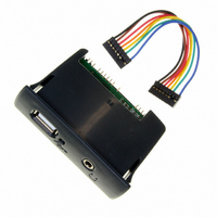
Manufacturer Part Number
VMUSIC2
Description
MOD USB FLASH DISK INTERFACE MP3
Manufacturer
FTDI, Future Technology Devices International Ltd
Series
-r
Datasheet
1.VMUSIC2.pdf
(8 pages)
Specifications of VMUSIC2
Accessory Type
USB Audio Module
Color
Black
For Use With/related Products
Audio Files on Thumbdrive
Lead Free Status / RoHS Status
Lead free / RoHS Compliant
Other names
768-1004


Ta�le �� � Data and Control ��us �ignal Mode �ptions � ��I Inter�ace
Figure 2 � ��I �lave Data �ead Cycle
From �tart � ��I C� must �e held high �or the entire read cycle�� and must �e taken low �or at least one clock period
����� �h� ���� �� �����p������ �h� ����� b�� �� S��I ���� I� �� �h� R/W b�� - ��p�����g � ‘1’ h��� ������ ���� �� b� ���� �����
the chip. The ne�t �it is the address �it�� ��DD�� which is used to indicate whether the data register (�0�) or the status
register (�1�) is read �rom. During the ��I read cycle a �yte o� data will start �eing output on ��I Data �ut on the ne�t
������k ��y���� ����� �h� ������� b���� MSB ������ ����� �h� ���� h�� b��� ������k�� ��� �� �h� ��h�p�� �h� ������ �� S��I ����
�ut should �e checked to see i� the data read is new data. �� �0� level here on ��I Data �ut means that the data read
is new data. �� �1� indicates that the data read is old data�� and the read cycle should �e repeated to get new data.
�emem�er that C� must �e held low �or at least one clock period �e�ore �eing taken high again to continue with the
ne�t read or write cycle.
Figure �� � ��I �lave Data Write Cycle
From �tart � ��I C� must �e held high �or the entire write cycle�� and must �e taken low �or at least one clock period
����� �h� ����� �� �����p������ �h� ����� b�� �� S��I ���� I� �� �h� R/W b�� - ��p�����g � ‘0’ h��� ������ ���� �� b� �������
to the chip. The ne�t �it is the address �it�� ��DD�� which is used to indicate whether the data register (�0�) or the status
register (�1�) is written to. During the ��I write cycle a �yte o� data can �e input to ��I Data In on the ne�t clock cycle
����� �h� ������� b���� MSB ������ ����� �h� ���� h�� b��� ������k�� �� �� �h� ��h�p�� �h� ������ �� S��I ���� O�� �h���� b�
VMusic2 Vinculum VNC1L Module
SPI Data Out
SPI Data Out
Datasheet Version 0.98
Pin No.
�
4
2
6
SPI Data In
SPI Data In
SPI CS
SPI CS
SPICLK
SPICLK
2.3 SPI Interface Signal Descriptions and Timing Diagrams
Name
�CLK
�DI
�D�
C�
1
Type
Input
Input
�utput
Input
1
R/W ADD
0
R/W ADD
1
0
Description
��I Clock input�� 12MHz ma�imum.
��I �erial Data Input
��I �erial Data �utput
��I Chip �elect Input
0
D7
D7
D6
D5
D6
D4
D5
D3
D4
D2
D3
D1
D2
D0
© Future Technology Devices International Ltd. 2007
D1
D0
Page
Related parts for VMUSIC2
Image
Part Number
Description
Manufacturer
Datasheet
Request
R

Part Number:
Description:
IC USB TO SERIAL UART 32-QFN
Manufacturer:
FTDI, Future Technology Devices International Ltd

Part Number:
Description:
IC USB HOST CTLR VINCULUM 48LQFP
Manufacturer:
FTDI, Future Technology Devices International Ltd
Datasheet:

Part Number:
Description:
IC USB HOST VINCULUM-II 32QFN
Manufacturer:
FTDI, Future Technology Devices International Ltd
Datasheet:
Part Number:
Description:
IC USB HOST VINCULUM-II 32LQFN
Manufacturer:
FTDI, Future Technology Devices International Ltd
Datasheet:
Part Number:
Description:
IC USB HOST VINCULUM-II 48QFN
Manufacturer:
FTDI, Future Technology Devices International Ltd
Datasheet:
Part Number:
Description:
IC USB HOST VINCULUM-II 32LQFN
Manufacturer:
FTDI, Future Technology Devices International Ltd
Datasheet:
Part Number:
Description:
IC USB HOST VINCULUM-II 32QFN
Manufacturer:
FTDI, Future Technology Devices International Ltd
Datasheet:
Part Number:
Description:
IC USB HOST VINCULUM-II 48LQFP
Manufacturer:
FTDI, Future Technology Devices International Ltd
Datasheet:
Part Number:
Description:
IC USB HOST VINCULUM-II 48LQFP
Manufacturer:
FTDI, Future Technology Devices International Ltd
Datasheet:
Part Number:
Description:
IC USB HOST VINCULUM-II 48QFN
Manufacturer:
FTDI, Future Technology Devices International Ltd
Datasheet:
Part Number:
Description:
IC USB HOST CTLR VINCULUM 64QFN
Manufacturer:
FTDI, Future Technology Devices International Ltd
Datasheet:

Part Number:
Description:
IC USB HOST CTLR VINCULUM 64LQFP
Manufacturer:
FTDI, Future Technology Devices International Ltd
Datasheet:
Part Number:
Description:
IC USB HOST VINCULUM-II 64LQFP
Manufacturer:
FTDI, Future Technology Devices International Ltd
Datasheet:
Part Number:
Description:
IC USB HOST VINCULUM-II 64QFN
Manufacturer:
FTDI, Future Technology Devices International Ltd
Datasheet:

Part Number:
Description:
IC USB TO PARALLEL FIFO 28-SSOP
Manufacturer:
FTDI, Future Technology Devices International Ltd
Datasheet: