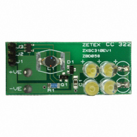
ZXSC310EV Diodes Zetex, ZXSC310EV Datasheet
ZXSC310EV
Specifications of ZXSC310EV


Related parts for ZXSC310EV


ZXSC310EV Summary of contents
Page 1
LED DRIVER SOLUTION FOR LCD BACKLIGHTING DEVICE DESCRIPTION The ZXSC310 is a single or multi cell LED driver designed for LCD backlighting applications. The input voltage range of the device is between 0.8V and 8V. This means the ZXSC310 is ...
Page 2
ZXSC310 ABSOLUTE MAXIMUM RATINGS: Supply Voltage Maximum Voltage other pins Power Dissipation Operating Temperature Storage Temperature ELECTRICAL CHARACTERISTICS: Test conditions unless otherwise stated: V Symbol Parameter (1) Efficiency V Recommended supply CC voltage range V Minimum startup and CC(min) operating ...
Page 3
FMMT618 For the circuits described in the applications section Zetex FMMT618 is the recommended pass transistor. ELECTRICAL CHARACTERISTICS: Test conditions unless otherwise stated: T Symbol Parameter V Collector-Emitter CE(sat) 5 Saturation Voltage V Collector-Emitter (BR)CEO Breakdown Voltage 5 Measured under ...
Page 4
ZXSC310 TYPICAL CHARACTERISTICS ISSUE 3 - SEPTEMBER 2007 4 ...
Page 5
DEVICE DESCRIPTION The ZXSC310 is PFM, controller IC which, when combined with a high performance external transistor, enables the production of a high efficiency boost converter for LED driving applications. A block diagram is shown for the ZXSC310 below. The ...
Page 6
ZXSC310 REFERENCE DESIGNS Three typical LED driving applications are shown. Firstly a typical LCD backlight circuit, then maximum brightness LED driving solution and lastly an optimised battery life LED driving solution. LCD backlight circuit ...
Page 7
Maximum brightness solution L1 V BATT FMMT617 CC V DRIVE S TDN I SENSE ZXSC310 This circuit provides a continuous current output to the LED by rectifying and buffering the DC-DC output. This ensures ...
Page 8
ZXSC310 Maximum battery life solution To ensure optimum efficiency, and therefore maximum battery life, the LED is supplied with a pulsed current. Maximum efficiency is ensured with the removal of rectifier losses experienced in the maximum brightness solution. Materials list ...
Page 9
APPLICATIONS INFORMATION The following section is a design guide for optimum converter performance. Switching transistor selection The choice of switching transistor has a major impact on the converter efficiency. For optimum performance, a bipolar transistor with low V CE(SAT) required. ...
Page 10
ZXSC310 Peak current definition The peak current rating is a design parameter whose value is dependent upon the overall application. For the high brightness reference designs, a peak current of 190mA was chosen to ensure that the converter could provide ...
Page 11
Output Power Calculation By making the above assumptions for inductance and peak current the output power can be determined by: T OFF = − × × OUT OUT ...
Page 12
ZXSC310 Shutdown Control The ZXSC310 offers a shutdown mode that produces a standby current of less than 5uA when in operation. When the voltage at the S pin is 0.7V or higher the TDN ZXSC310 is enabled, hence the driver ...
Page 13
PINOUT DIAGRAM VCC STDN PIN DESCRIPTIONS Pin No. Name TDN 4 I Inductor current sense input. Internal threshold voltage set to 19mV. SENSE 5 V Drive output for external switching transistor. Connect ...
Page 14
ZXSC310 (NOTES ISSUE 3 - SEPTEMBER 2007 14 ...
Page 15
Definitions Product change Zetex Semiconductors reserves the right to alter, without notice, specifications, design, price or conditions of supply of any product or service. Customers are solely responsible for obtaining the latest relevant information before placing orders. Applications disclaimer The ...
Page 16
ZXSC310 SOT23-5 PACKAGE OUTLINE © Zetex Semiconductors plc 2007 Europe Americas Zetex GmbH Zetex Inc Kustermannpark 700 Veterans Memorial Hwy Balanstraße 59 Hauppauge, NY 11788 D-81541 München USA Germany Telefon: (49 Telephone: (1) 631 360 ...