SYNC SEPARATOR AND DC RESTORATION AMPLIFIER
EVALUATION BOARD
Evaluation board description
This evaluation board has been developed to allow the
user to quickly evaluate the ZXFV4583 Sync separator
IC and the ZXFV4089 dc restoration video amplifier.
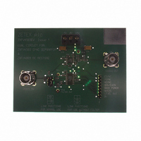
The evaluation board schematic diagram is shown in
Figure 1, and the printed circuit layout is shown in
Figures 2, 3 and 4.
The analog video source is brought onto the board via
a BNC connector socket and is terminated via a 51
resistor. This provides matching to standard
laboratory test instruments. The circuit can be easily
adapted for 75
resistor R1.
The incoming video signal is ac coupled to the
ZXFV4583 via capacitor C1 and is ac coupled to the
ZXFV4089 by capacitor C7.
Header PL2 in conjunction with links LK1 and LK2 allow
the incoming video signal to be passed through the
internal color burst filter or to bypass it.
To use the color burst filter:
Links LK1 should be connected between PL2:1 and PL2:6
Link LK2 should be connected between PL2:4 and PL2:5
To bypass the color burst filter:
Links LK1 should be connected between PL2:2 and PL2:5
Link LK2 should be connected between PL2:3 and PL2:4
Test point TP2 has been provided to monitor the output
of the color burst filter.
Diagrams of this are shown on the PCB itself.
The synchronized logic outputs of the ZXFV4583 are
brought to header H1 for examination using
oscilloscope probes
The ZXFV4089 DC Restoration Amplifier, which is
described in its own datasheet, uses the Back Porch
output from the ZXFV4583 in order to control and
stabilize the black level of a video waveform.
ISSUE 1 - MAY 2004
source impedance by changing
1
The ZXFV4089 contains an uncommitted current
feedback amplifier. This evaluation board uses
resistors R7 and R8 to set the gain of this amplifier. The
default gain setting of the evaluation board is +2 or
6.02dB.
The output circuit includes a resistor matching circuit
to present a load of 150
simultaneously providing a 50
any test instrument connected to the BNC connector.
The attenuation of this matching circuit is 19.92dB. This
results in an overall gain for a 50
6.02 - 19.92 = -13.9dB.
PCB design
A continuous ground plane is required under the
device and its signal connection paths, to provide the
shortest possible ground return paths for signals and
power supply filtering.
A double-sided or multi-layer PCB construction is
required, with plated-through via holes providing
closely spaced low-inductance connections from some
components to the continuous ground plane.
Power supply filtering
For the power supply filtering, low inductance surface
mount capacitors are normally required. It has been
found that very good RF decoupling is provided on
each supply using a 1000pF NPO size 0805 or smaller
ceramic surface mount capacitor, closest to the device
pin, with an adjacent 0.1 F X7R capacitor. However
larger decoupling capacitors elsewhere on the printed
circuit board, values of 1 to 10 F, are also
recommended, particularly where the voltage
regulators are located more than a few inches from the
device. These larger capacitors are recommended to
be solid tantalum electrolytic or ceramic types
ZXFV4583EV
to the amplifier while
output impedance to
S E M I C O N D U C T O R S
system of:
.