ECLSOIC8EVB ON Semiconductor, ECLSOIC8EVB Datasheet
ECLSOIC8EVB
Specifications of ECLSOIC8EVB
ECLSOIC8EVBOS


Related parts for ECLSOIC8EVB

ECLSOIC8EVB Summary of contents
Page 1
... The FR4 dielectric material is EE placed between second and third layer and between third and fourth layer. The third layer is also 1.0 oz copper ground plane and a portion of this layer is V fourth layer is the secondary trace layer. 1 power plane. The CC Publication Order Number: ECLSOIC8EVB/D ...
Page 2
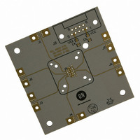
... The input, output, and power pin layout of the evaluation board is shown in Figure 3. The evaluation board has at least eleven possible configurable options. Table 1. list the Top View ECLSOIC8EVB LAY−UP DETAIL 4 LAYER LAYER 1 (TOP SIDE) ROGERS 4003 0.008 in FR− ...
Page 3
... See Figure 6 MC100LVEL12D See Figure 6 MC100LVEL16D* See Figure 5 MC100LVEL31D See Figure 4 MC100LVEL32D See Figure 7 MC100LVEL33D See Figure 7 MC100LVEL51D See Figure 4 MC100LVEL58D See Figure 8 MC100LVELT22D See Figure 11 MC100LVELT23D See Figure 12 ECLSOIC8EVB Device Configuration MC10EP01D/MC100EP01D 1 MC10EP05D/MC100EP05D 2 MC10EP08D/MC100EP08D 1 MC10EP11D/MC100EP11D 2 MC10EP16D/ 3 MC100EP16D* 3 MC100EP16FD* 2 MC10EP16TD/ 1 MC100EP16TD* ...
Page 4
... Table 3. Power Supply Levels for Translators V CC PECL Translators 3 5.0 V ECLSOIC8EVB On the top side of the evaluation board solder the four surface mount test point clips to the pads labeled V and GND. The V device. The V There are two GND clip footprints which can be connected to the ground plane of the evaluation board depending on the setup configuration ...
Page 5
... CONFIGURATIONS Table 4. Configuration 1 J1 Device MC10EL01D/MC100EL01D MC10EL05D/MC100EL05D MC10EL31D/MC100EL31D MC10EL35D/MC100EL35D MC10EL51D/MC100EL51D MC10EL52D/MC100EL52D MC100LVEL01D MC100LVEL05D MC100LVEL31D Yes MC100LVEL51D MC10EP01D/MC100EP01D MC10EP05D/MC100EP05D MC10EP08D/MC100EP08D MC10EP31D/MC100EP31D MC10EP35D/MC100EP35D MC10EP51D/MC100EP51D MC10EP52D/MC100EP52D ECLSOIC8EVB DUT Figure 4. Configuration 1 Schematic Pin 1 Pin 2 Pin 3 Pin Yes Yes Yes Yes Yes Yes Yes http://onsemi.com ...
Page 6
... J4 (Optional) Table 5. Configuration 2 Device MC10EL04D/MC100EL04D MC10EL07D/MC100EL07D MC10EL16D/MC100EL16D* MC100LVEL16D* MC10EP16D/MC100EP16D* MC100EP16FD* MC100LVEP160* MC10EP16TD/MC100EP16TD* MC100EP16VAD* MC100EP16VBD* MC100EP16VSD* MC100EP16VTD* NB6L160D *See Appendix for additional or modification to the current configuration ECLSOIC8EVB V CC Pin 1 Pin 8 Pin 7 Pin DUT Pin 3 Pin Pin 4 Pin 5 V Figure 5. Configuration 2 Schematic Pin 1 ...
Page 7
... Table 6. Configuration 3 Device MC10EL11D/MC100EL11D MC10EL12D/MC100EL12D MC10EL89D/MC100EL89D MC100LVEL11D MC100LVEL12D MC10EP11D/MC100EP11D MC100EP89D MC100LVEP11D NB6L11D ECLSOIC8EVB Pin 1 Pin 8 Pin 7 Pin 2 DUT Pin 3 Pin 6 Pin 4 Pin 5 Figure 6. Configuration 3 Schematic Pin 1 Pin 2 Pin 3 Pin Yes No Yes No Yes No Yes http://onsemi.com 7 V GND GND ...
Page 8
... (Optional) Table 7. Configuration 4 J1 Device MC10EL32D/MC100EL32D MC10EL33D/MC100EL33D MC100LVEL32D Yes Yes MC100LVEL33D MC10EP32D/MC100EP32D MC10EP33D/MC100EP33D ECLSOIC8EVB V CC Pin 1 Pin Pin 7 Pin DUT Pin 3 Pin Pin 4 Pin Figure 7. Configuration 4 Schematic Pin 1 Pin 2 Pin 3 Pin Yes Yes Yes Yes Yes Yes Yes Yes Yes Yes ...
Page 9
... (Optional) Table 8. Configuration 5 Device MC100EP16VCD* MC10EL58D/MC100EL58D MC100LVEL58D MC10EP58D/MC100EP58D *See Appendix for addition or modification to the current configuration ECLSOIC8EVB V Pin 1 Pin 8 R2 Pin 7 Pin DUT Pin 3 Pin Pin 4 Pin Figure 8. Configuration 5 Schematic Pin 1 Pin 2 Pin 3 Pin Yes Yes Yes Yes Yes Yes No No ...
Page 10
... J2 J3 Figure 9. Configuration 6 − Translator Schematic Table 9. Configuration 6 Pin Device MC10ELT20D/MC100EL20D MC10EPT20D/MC100EPT20D ECLSOIC8EVB 0.1 mF Pin 1 Pin 8 C1 0.01 mF Pin 7 Pin DUT (optional) J7 Pin 3 Pin 6 Pin 4 Pin 5 Short V EE Pin 2 Pin 3 Pin 4 Pin Yes Yes No No Yes Yes http://onsemi.com 10 GND GND ...
Page 11
... J2 J3 Figure 10. Configuration 7 − Translator Schematic Table 10. Configuration 7 Device MC10ELT21D/MC100EL21D MC100EPT21D *See Appendix for loaded testing condition. ECLSOIC8EVB Pin 1 Pin 8 Pin 7 Pin DUT Pin 3 Pin Pin 4 Pin 5 (Unloaded Testing Condition) Pin 1 Pin 2 Pin 3 Pin Yes Yes Yes Yes Yes Yes Yes ...
Page 12
... Figure 11. Configuration 8 − Translator Schematic Table 11. Configuration 8 Pin Device MC10ELT22D/ MC100EL22D Yes MC100LVELT22D MC100EPT22D ECLSOIC8EVB V Pin 1 Pin 8 Pin 7 Pin 2 DUT Pin 3 Pin 6 Pin 4 Pin 5 Pin 2 Pin 3 Pin 4 Pin Yes Yes No N Yes http://onsemi.com 12 GND (optional (optional) Short V GND ...
Page 13
... Figure 12. Configuration 9 − Translator Schematic Table 12. Configuration 9 Device MC100EL23D MC100LVELT23D MC100EPT23D *See Appendix for loaded testing condition. ECLSOIC8EVB V Pin 1 Pin Pin 7 Pin DUT Pin 3 R3 Pin Pin 4 R4 Pin (Unloaded Testing Condition) Pin 1 Pin 2 Pin 3 Pin Yes Yes Yes Yes Yes ...
Page 14
... J2 J3 Figure 13. Configuration 10 − Translator Schematic Table 13. Configuration 10 Device MC10ELT26D/MC100ELT26D MC100EPT26D *See Appendix for loaded testing condition. ECLSOIC8EVB Pin 1 Pin 8 Pin 7 Pin DUT Pin 3 R3 Pin Pin 4 Pin 5 (Unloaded Testing Condition) Pin 1 Pin 2 Pin 3 Pin Yes Yes Yes Yes Yes Yes ...
Page 15
... Figure 14. Configuration 11 − Translator Schematic Table 14. Configuration 11 Pin Device MC10ELT28D/MC100ELT28D Yes Yes ECLSOIC8EVB 0.1 mF Pin 1 Pin 0.01 mF Pin 7 Pin DUT Pin 3 R6 Pin (optional) Pin 4 Pin 5 Short V EE Pin 2 Pin 3 Pin 4 Pin Yes Yes Yes No Yes No No http://onsemi.com 15 GND J7 J6 ...
Page 16
... ECL signals (V – 2 split power supply setup, V system ground 2.0 V, and V CC –1.3 V; see Table 15). Table 15. Power Supply Levels Power Supply V CC 5.0 V 2.0 V 3.3 V 2.0 V 2.5 V 2.0 V ECLSOIC8EVB Power Supply V GND DUT GND EE Power Supply , V ...
Page 17
... Compact Test Point 0603 0.01 mF 10% 06035C103KAT2A 0603 0.1 mF 10% 06035C104KAT2A 0603 Thick CRCW060351R1J Film Resistor SOIC 8 Evaluation Board ECLSOIC8EVB SOIC 8 Package Device Various http://onsemi.com 17 Web Site http://www.rosenberger.de http://www.rosenbergerna.com http://www.johnsoncomponents.com http://www.keyelco.com http://www.avxcorp.com http://www.vishay.com http://www ...
Page 18
... To utilize the feedback option and enable option, Configuration 5 needs to be modified. 1. Connect a SMA connector on J1. 2. Remove the 50 W chip resistor from R3. ECLSOIC8EVB MC100EP16VSD This device has an option of varying the output swing amplitude and being driven single−endedly. In order to utilize these options, Configuration 2 needs to be modified ...
Page 19
... Appendix B (Gerber Files) Top Layer Third Layer (V and Ground Plane) CC ECLSOIC8EVB Second Layer (V Bottom Layer Figure 16. Gerber Files http://onsemi.com 19 and Ground Plane EE ...
Page 20
... USA/Canada Japan: ON Semiconductor, Japan Customer Focus Center 2−9−1 Kamimeguro, Meguro−ku, Tokyo, Japan 153−0051 Phone: 81−3−5773−3850 http://onsemi.com 20 ON Semiconductor Website: http://onsemi.com Order Literature: http://www.onsemi.com/litorder For additional information, please contact your local Sales Representative. ECLSOIC8EVB/D ...