NBSG11BAEVB ON Semiconductor, NBSG11BAEVB Datasheet - Page 5
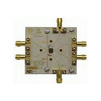
NBSG11BAEVB
Manufacturer Part Number
NBSG11BAEVB
Description
BOARD EVALUATION BBG NBSG11BA
Manufacturer
ON Semiconductor
Specifications of NBSG11BAEVB
Technology Type
Evaluation Board
Lead Free Status / RoHS Status
Contains lead / RoHS non-compliant
For Use With/related Products
NBSG11
Other names
NBSG11BAEVB
NBSG11BAEVBOS
NBSG11BAEVBOS


Setup Test Configurations For Differential Operation
Small Signal Setup
Step 2:
Large Signal Setup
Step 2:
Step 3:
Step 3:
Input Setup
Output Setup
Input Setup
Output Setup
50 W
2a: Calibrate VNA from 1.0 GHz to 12 GHz.
2b: Set input level to –35 dBm at the output of the 180 Hybrid coupler (input of the DUT).
3a: Set display to measure S21 and record data.
2a: Calibrate VNA from 1.0 GHz to 12 GHz.
2b: Set input levels to -2.0 dBm (500 mV) at the input of DUT.
3a: Set display to measure S21 and record data.
GND
Coupler
NOTE:
Hybrid
PORT 1
Hybrid Coupler has equal power split
(3dB) with 180 between outputs
Figure 4. NBSG11 Board Setup – Frequency Domain
CLK
CLK
V
EE
= -1.3 V (3.3 V op)
Vector Network Analyzer
NBSG11BAEVB
http://onsemi.com
(Differential Mode)
Rohde & Schwartz
V
V
V
CC
CC
EE
= 2.0 V
5
Q1
Q0
GND
GND
50 W
V
V
TT
TT
Q0
Q1
GND
GND
= 0 V
= 0 V
Bias T
GND
50 W
GND
PORT 2
50 W
Related parts for NBSG11BAEVB
Image
Part Number
Description
Manufacturer
Datasheet
Request
R

Part Number:
Description:
Buffers & Line Drivers 2.5V/3.3V Multilevel
Manufacturer:
ON Semiconductor

Part Number:
Description:
ON Semiconductor [VOLTAGE REGULATOR]
Manufacturer:
ON Semiconductor
Datasheet:
Part Number:
Description:
357-036-542-201 CARDEDGE 36POS DL .156 BLK LOPRO
Manufacturer:
ON Semiconductor
Datasheet:
Part Number:
Description:
357-036-542-201 CARDEDGE 36POS DL .156 BLK LOPRO
Manufacturer:
ON Semiconductor
Datasheet:
Part Number:
Description:
357-036-542-201 CARDEDGE 36POS DL .156 BLK LOPRO
Manufacturer:
ON Semiconductor
Datasheet:
Part Number:
Description:
357-036-542-201 CARDEDGE 36POS DL .156 BLK LOPRO
Manufacturer:
ON Semiconductor
Datasheet:
Part Number:
Description:
357-036-542-201 CARDEDGE 36POS DL .156 BLK LOPRO
Manufacturer:
ON Semiconductor
Datasheet:
Part Number:
Description:
357-036-542-201 CARDEDGE 36POS DL .156 BLK LOPRO
Manufacturer:
ON Semiconductor
Datasheet:
Part Number:
Description:
357-036-542-201 CARDEDGE 36POS DL .156 BLK LOPRO
Manufacturer:
ON Semiconductor
Datasheet:
Part Number:
Description:
357-036-542-201 CARDEDGE 36POS DL .156 BLK LOPRO
Manufacturer:
ON Semiconductor
Datasheet:
Part Number:
Description:
357-036-542-201 CARDEDGE 36POS DL .156 BLK LOPRO
Manufacturer:
ON Semiconductor
Datasheet:
Part Number:
Description:
357-036-542-201 CARDEDGE 36POS DL .156 BLK LOPRO
Manufacturer:
ON Semiconductor
Datasheet:
Part Number:
Description:
Manufacturer:
ON Semiconductor
Datasheet: