AD8225-EVAL Analog Devices Inc, AD8225-EVAL Datasheet - Page 4
AD8225-EVAL
Manufacturer Part Number
AD8225-EVAL
Description
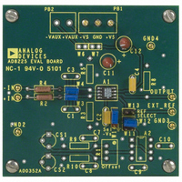
BOARD EVAL FOR AD8225
Manufacturer
Analog Devices Inc
Specifications of AD8225-EVAL
Lead Free Status / RoHS Status
Contains lead / RoHS non-compliant


AD8225
SPECIFICATIONS
Parameter
GAIN
OFFSET VOLTAGE (RTI)
INPUT
OUTPUT
DYNAMIC RESPONSE
NOISE (RTI)
REFERENCE INPUT
POWER SUPPLY
TEMPERATURE RANGE
*Pin 1 connected to Pin 4. See Applications section.
Specifications subject to change without notice.
Gain
Gain Error
Nonlinearity
vs. Temperature
Offset Voltage
vs. Temperature
vs. Supply
Input Operating Impedance
Input Voltage Range
(Common-Mode)
Input Bias Current
Input Offset Current
Common-Mode Rejection Ratio
Operating Voltage Range
Operating Voltage Range
Short Circuit Current
Small Signal –3 dB Bandwidth
Full Power Bandwidth
Settling Time (0.01%)
Settling Time (0.001%)
Slew Rate
Voltage
Current
R
I
Voltage Range
Gain to Output
Operating Range
Quiescent Current
For Specified Performance
IN
IN
Differential
Common Mode
vs. Temperature
vs. Temperature
vs. Temperature
vs. Temperature
vs. Temperature
(T
A
= 25 C, V
Conditions
T
f = 10 kHz*
R
R
V
2 V Step
2 V Step
0.1 Hz to 10 Hz
Spectral Density, 1 kHz
0.1 Hz to 10 Hz
Spectral Density, 1 kHz
L
L
OUT
A
= 2 kΩ
= 10 kΩ
= T
= 3.2 V p-p
S
MIN
= 5 V, R
to T
L
MAX
= 2 k , unless otherwise noted.)
–4–
Min
–0.1
90
1.6
1.7
86
83
80
0.8
0.9
0.8
0.9
5
0.4
0.999
3.4
–40
Typ
5
+0.05
2
1
150
100
10 2
10 2
0.5
3
0.15
1.5
94
18
900
420
3.3
5.1
1.5
45
4
50
18
60
1
1.05
Max
+0.1
10
5
375
2
V
V
0.5
V
V
V
V
V
1.001
36
1.2
+85
1.2
S
S
S
S
S
S
S
– 1.05
– 1.0
– 1.05
– 1.2
– 1.0
– 1.0
– 0.9
Unit
V/V
%
± ppm
± ppm/°C
±µV
±µV/°C
dB
GΩ pF
GΩ pF
V
V
nA
pA/°C
nA
pA/°C
dB
dB
dB
V
V
V
V
mA
kHz
kHz
µs
µs
V/µs
µV p-p
nV/√Hz
pA p-p
fA/√Hz
kΩ
µA
V
V
mA
°C
REV. A
Related parts for AD8225-EVAL
Image
Part Number
Description
Manufacturer
Datasheet
Request
R

Part Number:
Description:
BOARD EVAL FOR AD8225 INSTR AMP
Manufacturer:
Analog Devices Inc
Datasheet:

Part Number:
Description:
±1.7g Dual-Axis IMEMS Accelerometer Evaluation Board
Manufacturer:
Analog Devices Inc
Datasheet:
Part Number:
Description:
Inertial Sensor Evaluation System
Manufacturer:
Analog Devices Inc
Datasheet:
Part Number:
Description:
Manufacturer:
Analog Devices Inc
Datasheet:
Part Number:
Description:
Manufacturer:
Analog Devices Inc
Datasheet:
Part Number:
Description:
Manufacturer:
Analog Devices Inc
Datasheet:
Part Number:
Description:
Manufacturer:
Analog Devices Inc
Datasheet:
Part Number:
Description:
Manufacturer:
Analog Devices Inc
Datasheet:
Part Number:
Description:
Manufacturer:
Analog Devices Inc
Datasheet:
Part Number:
Description:
Manufacturer:
Analog Devices Inc
Datasheet:
Part Number:
Description:
Manufacturer:
Analog Devices Inc
Datasheet:
Part Number:
Description:
Manufacturer:
Analog Devices Inc
Datasheet:
Part Number:
Description:
Manufacturer:
Analog Devices Inc
Datasheet: