AD9777-EB Analog Devices Inc, AD9777-EB Datasheet
AD9777-EB
Specifications of AD9777-EB


Related parts for AD9777-EB


AD9777-EB Summary of contents
Page 1
... MSPS 2x/4x/8x D/A Converter ® IDAC COS GAIN DAC SIN IMAGE REJECTION/ I/Q DAC DUAL DAC GAIN/OFFSET MODE REGISTERS BYPASS MUX SIN COS IDAC ) DIFFERENTIAL CLK © 2006 Analog Devices, Inc. All rights reserved. AD9777 OFFSET DAC I OUT www.analog.com ...
Page 2
... AD9777 TABLE OF CONTENTS Features .............................................................................................. 1 Applications....................................................................................... 1 General Description ......................................................................... 4 Product Highlights ....................................................................... 4 Specifications..................................................................................... 5 DC Specifications ......................................................................... 5 Dynamic Specifications ............................................................... 6 Digital Specifications ................................................................... 7 Digital Filter Specifications ......................................................... 8 Absolute Maximum Ratings............................................................ 9 Thermal Characteristics .............................................................. 9 ESD Caution.................................................................................. 9 Pin Configuration and Function Descriptions........................... 10 Terminology .................................................................................... 12 Typical Performance Characteristics ........................................... 13 Mode Control (via SPI Port)..................................................... 18 Register Description................................................................... 20 Functional Description ...
Page 3
... Edits to Figure 21 .......................................................................... 25 Edits to PLL Disabled, Two-Port Mode Section ....................... 25 Edits to Figure 22 .......................................................................... 25 Edits to Figure 23 .......................................................................... 26 Edits to Figure 26a ........................................................................ 27 Changes to Figures 53 and 54...................................................... 38 Edits to Evaluation Board Section .............................................. 39 Changes to Figures 56 to 59......................................................... 40 Replaced Figures ............................................................ 42 Updated Outline Dimensions...................................................... 49 7/02—Revision 0: Initial Version Rev Page AD9777 ...
Page 4
... V to 3.5 V single supply. The 20 mA full-scale current can be reduced for lower power operation, and several sleep functions are provided to reduce power during idle periods. 12. On-chip voltage reference: The AD9777 includes a 1.20 V temperature compensated band gap voltage reference. 13. An 80-lead thin quad flat package, exposed pad (TQFP_EP). ...
Page 5
... Rev Page AD9777 Max Unit Bits LSB +6.5 LSB +0.025 % of FSR +1 FSR + FSR 20 mA +1.25 V kΩ 1.25 V kΩ ...
Page 6
... AD9777 DYNAMIC SPECIFICATIONS AVDD = 3.3 V, CLKVDD = 3.3 V, DVDD = 3.3 V, PLLVDD = MIN MAX transformer-coupled output, 50 Ω doubly terminated, unless otherwise noted. Table 2. Parameter DYNAMIC PERFORMANCE Maximum DAC Output Update Rate (f Output Settling Time (t ) (to 0.025 Output Rise Time (10% to 90%) 1 Output Fall Time (10% to 90%) ...
Page 7
... SDIO Output Logic 1 Voltage Logic 0 Voltage Logic 1 Current Logic 0 Current ) ) ) DS Rev Page mA, unless otherwise noted. OUTFS Min Typ Max 2 0.9 −10 +10 −10 + 0.75 1.5 2.25 0.5 1 1.5 2 0.9 −10 +10 −10 +10 5 DRVDD − 0.6 0 AD9777 Unit V V µA µ MHz µA µ ...
Page 8
... AD9777 DIGITAL FILTER SPECIFICATIONS Table 4. Half-Band Filter No. 1 (43 Coefficients) Tap Coefficient − −134 244 10 11, 33 −414 12 13, 31 673 14 15, 29 −1,079 16 17, 27 1,772 18 19, 25 −3,280 20 21, 23 10,364 22 16,384 Table 5. Half-Band Filter No. 2 (19 Coefficients) Tap Coefficient −120 438 −1,288 5,047 10 8,192 Table 6. Half-Band Filter No. 3 (11 Coefficients) ...
Page 9
... AVDD, DVDD, CLKVDD −4.0 AGND, DGND, CLKGND −0.3 AGND −0.3 AGND −1.0 DGND −0.3 DGND −0.3 CLKGND −0.3 CLKGND −0.3 DGND −0.3 −65 Rev Page AD9777 Max Unit +4.0 V +4.0 V +0.3 V AVDD + 0.3 V AVDD + 0.3 V DVDD + 0.3 V DVDD + 0.3 V CLKVDD + 0.3 V CLKVDD + 0.3 V DVDD + 0 ...
Page 10
... CLKVDD LPF CLKVDD CLKGND CLK+ CLK– CLKGND DATACLK/PLL_LOCK DGND DVDD P1B15 (MSB) P1B14 P1B13 P1B12 P1B11 P1B10 DGND DVDD P1B9 P1B8 CONNECT PIN AD9777 8 TxDAC+ 9 TOP VIEW (Not to Scale Figure 5. Pin Configuration Rev Page FSADJ1 FSADJ2 59 REFIO 58 RESET 57 SPI_CSB 56 SPI_CLK ...
Page 11
... In two-port mode, this pin becomes the Port 2 MSB. With the PLL disabled and the AD9777 in one-port mode, this pin becomes a clock output that runs at twice the input data rate of the I and Q channels. This allows the AD9777 to accept and demux interleaved I and Q data to the I and Q input registers. ...
Page 12
... AD9777 TERMINOLOGY Adjacent Channel Power Ratio (ACPR) A ratio in dBc between the measured power within a channel relative to its adjacent channel. Complex Image Rejection In a traditional two-part upconversion, two images are created around the second IF frequency. These images are redundant and have the effect of wasting transmitter power and system bandwidth. ...
Page 13
... OUT DATA MSPS DATA MSPS DATA Rev Page 100 FREQUENCY (MHz MSPS with f DATA 90 0dBFS –6dBFS 70 –12dBFS FREQUENCY (MHz) Figure 10. In-Band SFDR vs MSPS OUT DATA 90 0dBFS 85 –12dBFS –6dBFS FREQUENCY (MHz) Figure 11. Out-of-Band SFDR vs OUT DATA AD9777 150 = f /3 OUT DATA MSPS ...
Page 14
... AD9777 10 0 –10 –20 –30 –40 –50 –60 –70 –80 –90 0 100 200 FREQUENCY (MHz) Figure 12. Single-Tone Spectrum @ f = 160 MSPS with f DATA 90 0dBFS –6dBFS –12dBFS FREQUENCY (MHz) Figure 13. In-Band SFDR vs OUT –6dBFS –12dBFS 70 65 0dBFS FREQUENCY (MHz) Figure 14. Out-of-Band SFDR vs. f OUT ...
Page 15
... AVDD ( 320 MSPS 160 MSPS DAC DATA PLL OFF PLL 100 INPUT DATA RATE (MSPS) Figure 22. SNR vs. Data Rate for MHz OUT 78MSPS f = 65MSPS DATA 160MSPS – TEMPERATURE (°C) Figure 23. SFDR vs. Temperature @ OUT AD9777 3 MHz, OUT 150 100 /11 DATA ...
Page 16
... AD9777 0 –10 –20 –30 –40 –50 –60 –70 –80 –90 –100 0 50 100 FREQUENCY (MHz) Figure 24. Single-Tone Spurious Performance 150 MSPS, No Interpolation DATA 0 –20 –40 –60 –80 –100 FREQUENCY (MHz) Figure 25. Two-Tone IMD Performance 150 MSPS, No Interpolation DATA 0 –10 –20 –30 – ...
Page 17
... FREQUENCY (MHz) Figure 30. Single-Tone Spurious Performance MSPS, Interpolation = 8× DATA 0 –10 –20 –30 –40 –50 –60 –70 –80 –90 –100 400 MHz, Figure 31. Eight-Tone IMD Performance, f OUT Rev Page AD9777 FREQUENCY (MHz) = 160 MSPS, Interpolation = 8x DATA ...
Page 18
... AD9777 MODE CONTROL (VIA SPI PORT) 1 Table 9. Mode Control via SPI Port Address Bit 7 Bit 6 00h SDIO LSB, MSB First Bidirectional 0 = MSB 0 = Input 1 = LSB 1 = I/O 01h Filter Filter Interpolation Interpolation Rate Rate (1×, 2×, (1×, 2×, 4×, 8×) 4×, 8×) 02h ...
Page 19
... QDAC Coarse Gain Adjustment QDAC QDAC Offset QDAC Offset Offset Adjustment Adjustment Adjustment Bit 6 Bit 5 Bit 7 Version Register Rev Page AD9777 Bit 2 Bit 1 Bit 0 QDAC QDAC QDAC Coarse Gain Coarse Gain Coarse Gain Adjustment Adjustment Adjustment QDAC Offset QDAC QDAC Adjustment ...
Page 20
... Bit 6: Logic 0 (default) places the AD9777 in two-port mode. I and Q data enters the AD9777 via Ports 1 and 2, respectively. A Logic 1 places the AD9777 in one-port mode in which interleaved I and Q data is applied to Port 1. See Table 8 for detailed information on how to use the DATACLK/PLL_LOCK, IQSEL, and ONEPORTCLK modes ...
Page 21
... Logic 1 applies a positive offset current OUTA . The magnitude of the offset current is defined by the and function of fine gain, OUTA OUTB is created by a single FSADJ resistor REF ⎤ ⎞ ⎟ ⎥ ⎠ ⎦ ⎤ ⎞ − 1 ⎟ ⎟ ⎥ ⎥ ⎠ ⎦ AD9777 (1) ...
Page 22
... GENERAL OPERATION OF THE SERIAL INTERFACE There are two phases to a communication cycle with the AD9777. Phase 1 is the instruction cycle, which is the writing of an instruction byte into the AD9777 coincident with the first eight SCLK rising edges. The instruction byte provides the ...
Page 23
... LSB first bit in Register 0. The default is MSB first. When this bit is set active high, the AD9777 serial port is in LSB first format. In LSB first mode, the instruction byte and data bytes must be written from LSB to MSB. In LSB first mode, the serial port internal byte address generator increments for each byte of the multibyte communication cycle ...
Page 24
... Figure 34. Serial Register Interface Timing LSB First SCLK t t PWH PWL INSTRUCTION BIT 7 INSTRUCTION BIT 6 Figure 35. Timing Diagram for Register Write to AD9777 t DV DATA BIT N DATA BIT N–1 Figure 36. Timing Diagram for Register Read from AD9777 Rev Page DATA TRANSFER CYCLE DATA TRANSFER CYCLE ...
Page 25
... If the AD9777 is dc-coupled to an external modulator, this feature can be used to cancel the output offset on the AD9777 as well as the input offset on the modulator. Figure 42 shows a typical example of the effect that the offset control has on LO suppression ...
Page 26
... CLOCK INPUT CONFIGURATION The clock inputs to the AD9777 can be driven differentially or single-ended. The internal clock circuitry has supply and ground (CLKVDD, CLKGND) separate from the other supplies on the chip to minimize jitter from internal noise sources ...
Page 27
... Semiconductor. These networks depend on the assumed transmission line impedance and power supply voltage of the clock driver. Optimum performance of the AD9777 is achieved when the driver is placed very close to the AD9777 clock inputs, thereby negating any transmission line effects such as reflec- tions due to mismatch. ...
Page 28
... MSPS are due to the maximum input DATA data rate of the AD9777. However, maximum rates of less than 160 MSPS and all minimum f rates are due to maximum and mini- DATA mum speeds of the internal PLL VCO. Figure 48 shows typical performance of the PLL lock signal (Pin 8 or Pin 53) when the PLL is in the process of locking ...
Page 29
... In the 2×, (MOD. ON) two-port mode, data at the two input ports is latched into the AD9777 on every rising edge of the data rate clock (DATACLK). In addition, in the two-port mode, the AD9777 can be programmed to generate an externally available DATACLK for the purpose of data synchronization. This data rate clock can be 2× ...
Page 30
... When Pin 8 is used as a clock output (DATACLK), its frequency is equal to that of CLKIN. Data at the input ports is latched into the AD9777 on the rising edge of the CLKIN. Figure 52 shows the delay, t inherent between the rising edge of CLKIN and the rising edge of DATACLK, as well as the setup and hold requirements for the data at Ports 1 and 2 ...
Page 31
... CLKIN. Internal clock dividers in the AD9777 syn- thesize the DATACLK signal at Pin 8, which runs at the input data rate and can be used to synchronize the input data. Data is latched into input Port 1 and Port 2 of the AD9777 on the rising edge of DATACLK. DATACLK speed is defined as the speed of t CLKIN divided by the interpolation rate ...
Page 32
... The rate of interpolation is determined by the state of Control Register 01h, Bit 7 and Bit 6. Figure 2 to Figure 4 show the response of the digital filters when the AD9777 is set to 2×, 4×, and 8× modes. The frequency axes of these graphs have been normalized to the input data rate of the DAC. As the graphs show, the digital filters can provide greater than out-of-band rejection ...
Page 33
... Examples of sine and cosine modulation are given in Figure 58. /2 Figure 58. Baseband Signal, Amplitude Modulated with Sine and Cosine Carriers Rev Page –jωt Ae /2j SINUSOIDAL MODULATION DC –jωt Ae /2j –jωt –jω COSINUSOIDAL MODULATION DC AD9777 ...
Page 34
... AD9777 MODULATION, NO INTERPOLATION With Control Register 01h, Bit 7 and Bit 6 set to 00, the interpolation function on the AD9777 is disabled. Figure 59 to Figure 62 show the DAC output spectral characteristics of the AD9777 in the various modulation modes, all with the interpolation filters disabled. The modulation frequency is determined by the state of Control Register 01h, Bits 5 and 4 ...
Page 35
... MODULATION, INTERPOLATION = 2× With Control Register 01h, Bit 7 and Bit 6 set to 01, the interpolation rate of the AD9777 is 2×. Modulation is achieved by multiplying successive samples at the interpolation filter output by the sequence (+1, −1). Figure 63 to Figure 66 represent the spectral response of the AD9777 DAC output with 2× ...
Page 36
... AD9777 MODULATION, INTERMODULATION = 4× With Control Register 01h, Bit 7 and Bit 6 set to 10, the interpolation rate of the AD9777 is 4×. Modulation is achieved by multiplying successive samples at the interpolation filter output by the sequence (0, +1, 0, −1). The Effects of Digital Modulation on DAC Output Spectrum, Interpolation = 4x 0 – ...
Page 37
... Figure 71 to Figure 74 represent the spectral response of the AD9777 DAC output with 8× interpolation in the various modulation modes to a narrow band baseband signal. The Effects of the Digital Modulation on the DAC Output Spectrum, Interpolation = 8× ...
Page 38
... DAC This image may be the desired signal application using one of the various modulation modes in the AD9777. This roll- off of image frequencies can be seen in Figure 59 to Figure 74, where the effect of the interpolation and modulation rate is apparent as well. ...
Page 39
... It is important to remember that in this application (two baseband data channels), the image rejection is not dependent on the data at either of the AD9777 input channels. In fact, image rejection still occurs with either one or both of the AD9777 input channels active. Note that by changing the ...
Page 40
... AD9777 REAL CHANNEL (IN IMAGINARY CHANNEL (IN REAL QUADRATURE MODULATOR IMAGINARY COMPLEX MODULATION FREQUENCY QUADRATURE MODULATION FREQUENCY Q REAL CHANNEL (OUT) A/2 1 –F C –B/2J –F C COMPLEX IMAGINARY CHANNEL (OUT) MODULATOR –A/2J –F C B/2 –F C A/4 + B/4J A/4 – B/4J 2 –F Q –F – F – OUT – ...
Page 41
... Due to this 3 dB increase in signal amplitude, the real and imaginary inputs to the AD9777 must be kept at least 3 dB below full scale when operating with the complex modulator. Overranging in the complex modulator results in severe distortion at the DAC output ...
Page 42
... Figure 89 to Figure 96 show the measured response of the AD9777 and AD8345 given the complex input signal to the AD9777 in Figure 89. The data in these graphs was taken with a data rate of 12.5 MSPS at the AD9777 inputs. The interpolation rate of 4× or 8× gives a DAC output data rate of 50 MSPS or 100 MSPS ...
Page 43
... Figure 86. 2× Interpolation, Complex f /8 Modulation DAC –3.0 –2.0 –1.0 0 1.0 2.0 3.0 (LO (× ) OUT DATA Figure 87. 4× Interpolation, Complex f /8 Modulation DAC –6.0 –4.0 –2.0 0 2.0 4.0 6.0 (LO (× ) OUT DATA Figure 88. 8× Interpolation, Complex f /8 Modulation DAC AD9777 8.0 ...
Page 44
... FREQUENCY (MHz) Figure 89. AD9777, Real DAC Output of Complex Input Signal Near Baseband (Positive Frequencies Only), Interpolation = 4×, No Modulation in AD9777 0 –10 –20 –30 –40 –50 –60 –70 –80 –90 –100 750 760 ...
Page 45
... FREQUENCY (MHz) Figure 95. AD9777, Real DAC Output of Complex Input Signal Near Baseband (Positive Frequencies Only), Interpolation = 8×, Complex Modulation in AD9777 = +f 0 –10 –20 –30 –40 –50 –60 –70 –80 –90 –100 80 100 700 Figure 96. AD9777 Complex Output from Figure 95, Now Quadrature ...
Page 46
... For the typical situation, where I both equal 50 Ω, the equivalent circuit values become V R Note that the output impedance of the AD9777 DAC itself is greater than 100 kΩ and typically has no effect on the impedance of the equivalent output circuit. DIFFERENTIAL COUPLING USING A TRANSFORMER An RF transformer can be used to perform a differential-to- single-ended signal conversion, as shown in Figure 98 ...
Page 47
... R is necessary only if level shifting is OPT required on the op amp output. In Figure 99, AVDD, which is the positive analog supply for both the AD9777 and the op amp, is also used to level shift the differential output of the AD9777 to midsupply (that is, AVDD/2). INTERFACING WITH THE AD8345 QUADRATURE ...
Page 48
... PLL enabled and disabled. Refer to Figure 105 to Figure 114, the schematics, and the layout for the AD9777 evaluation board for the jumper locations described below. The AD9777 outputs can be configured for various applications by referring to the following instructions ...
Page 49
... TO USE PECL CLOCK DRIVER (U8), SOLDER JP41 AND JP42 AND REMOVE TRANSFORMER T1. Figure 102. Test Configuration for AD9777 in One-Port Mode with PLL Enabled, Signal Generator Frequency = One-Half Interleaved Input Data Rate, ONEPORTCLK = Interleaved Input Data Rate, DAC Output Data Rate = Signal Generator Frequency × Interpolation Rate ...
Page 50
... JP39 SHOULD BE SOLDERED. IF DATACLK/PLL_LOCK IS PROGRAMMED TO OUTPUT PIN 53, JP46 AND JP47 SHOULD BE SOLDERED. SEE THE TWO PORT DATA INPUT MODE SECTION FOR MORE INFORMATION. Figure 103. Test Configuration for AD9777 in Two-Port Mode with PLL Disabled, DAC Output Data Rate = Signal Generator Frequency, INPUT CLOCK NOTES 1 ...
Page 51
... RC0603 G2 ENBL G3 VPS1 VOUT LOIP VPS2 LOIN G4A G1B G4B G1A QBBN IBBN QBBP IBBP ADTL1-12 CC0603 Figure 105. AD8345 Circuitry on AD9777 Evaluation Board Rev Page RC0603 ADTL1-12 CC0805 AD9777 ...
Page 52
... AD9777 CC0603 RC0603 CC0603 RC1206 CC0603 RC0603 CC0605 Figure 106. AD9777 Clock, Power Supplies, and Output Circuitry Rev Page CC0805 ...
Page 53
... Figure 107. AD9777 Evaluation Board Input (A Channel) and Clock Buffer Circuitry Rev Page AD9777 ...
Page 54
... AD9777 Figure 108. AD9777 Evaluation Board Input (B Channel) and SPI Port Circuitry Rev Page ...
Page 55
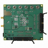
... Figure 109. AD9777 Evaluation Board Components, Top Side Figure 110. AD9777 Evaluation Board Components, Bottom Side Rev Page AD9777 ...
Page 56
... AD9777 Figure 112. AD9777 Evaluation Board Layout, Layer Two (Ground Plane) Figure 111. AD9777 Evaluation Board Layout, Layer One (Top) Rev Page ...
Page 57
... Figure 113. AD9777 Evaluation Board Layout, Layer Three (Power Plane) Figure 114. AD9777 Evaluation Board Layout, Layer Four (Bottom) Rev Page AD9777 ...
Page 58
... VIEW A ROTATED 90 ° CCW ORDERING GUIDE Model Temperature Range AD9777BSV −40°C to +85°C AD9777BSVRL −40°C to +85°C 1 AD9777BSVZ −40°C to +85°C 1 AD9777BSZVRL −40°C to +85°C AD9777- Pb-free part. 14.20 14.00 SQ 12.20 13.80 1.20 12.00 SQ MAX 11. PIN 1 TOP VIEW ...
Page 59
... NOTES Rev Page AD9777 ...
Page 60
... AD9777 NOTES © 2005 Analog Devices, Inc. All rights reserved. Trademarks and registered trademarks are the property of their respective owners. C02706-0-1/06(C) Rev Page ...