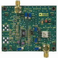
AD8331-EVAL Analog Devices Inc, AD8331-EVAL Datasheet - Page 29

AD8331-EVAL
Manufacturer Part Number
AD8331-EVAL
Description
BOARD EVAL FOR AD8331
Manufacturer
Analog Devices Inc
Specifications of AD8331-EVAL
Design Resources
Interfacing the High Frequency AD8331 to AD9215 (CN0096)
Module/board Type
Evaluation Board
For Use With/related Products
AD8331
Lead Free Status / RoHS Status
Contains lead / RoHS non-compliant
Output Clamping
Outputs are internally limited to a level of 4.5 V p-p differential
when operating at a 2.5 V common-mode voltage. The postamp
implements an optional output clamp engaged through a resistor
from R
resistor values.
Output clamping can be used for ADC input overload protection, if
needed, or postamp overload protection when operating from a
lower common-mode level, such as 1.5 V. The user should be
aware that distortion products increase as output levels approach
the clamping levels, and the user should adjust the clamp resistor
accordingly. For additional information, see the Applications
Information section.
The accuracy of the clamping levels is approximately ±5% in LO
or HI mode. Figure 80 illustrates the output characteristics for a
few values of R
CLMP
to ground. Table 8 shows a list of recommended
CLMP
.
Rev. G | Page 29 of 56
5.0
4.5
4.0
3.5
3.0
2.5
2.0
1.5
1.0
0.5
0
–3
R
8.8kΩ
3.5kΩ
3.5kΩ
8.8kΩ
Figure 80. Output Clamping Characteristics
CLMP
R
R
–2
= 1.86kΩ
CLMP
CLMP
=
=
∞
∞
AD8331/AD8332/AD8334
–1
V
INH
0
(V)
1
2
3


