AD9956/PCB Analog Devices Inc, AD9956/PCB Datasheet - Page 18
AD9956/PCB
Manufacturer Part Number
AD9956/PCB
Description
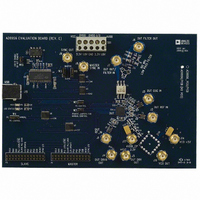
BOARD EVAL FOR AD9956
Manufacturer
Analog Devices Inc
Datasheet
1.AD9956YCPZ.pdf
(32 pages)
Specifications of AD9956/PCB
Module/board Type
Evaluation Board
For Use With/related Products
AD9956
Lead Free Status / RoHS Status
Contains lead / RoHS non-compliant


AD9956
GENERAL DESCRIPTION
DDS CORE
The DDS can create digital phase relationships by clocking a
48-bit accumulator. The incremental value loaded into the
accumulator, known as the frequency tuning word, controls the
overflow rate of the accumulator. Similar to a sine wave com-
pleting a 2π radian revolution, the overflow of the accumulator
is cyclical in nature and generates a base frequency according to
the following equation.
The instantaneous phase of the sine wave is, therefore, the out-
put of the phase accumulator block. This signal can be phase-
offset by programming an additive digital phase added to each
and every phase sample coming out of the accumulator.
These instantaneous phase values are then piped through a
phase-to-amplitude conversion (sometimes called an angle-
to-amplitude conversion or AAC) block. This algorithm follows
a COS(x) relationship where x is the phase coming out of the
phase offset block, normalized to 2π.
Finally, the amplitude words are piped to a 14-bit DAC. Because
the DAC is a sampled data system, the output is a reconstructed
sine wave that needs to be filtered to take high frequency
images out of the spectrum. The DAC is a current-steering
DAC that is AVDD referenced. To get a measurable voltage
output, the DAC outputs must terminate through a load resistor
to AVDD, typically 50 Ω. At positive full scale, IOUT sinks no
current and the voltage drop across the load resistor is zero.
However, the IOUT output sinks the DAC’s programmed full-
scale output current, causing the maximum output voltage to
drop across the load resistor. At negative full-scale, the situation
is reversed and IOUT sinks the full-scale current (and generates
the maximum drop across the load resistor). At the same time,
IOUT sinks no current (and generates no voltage drop). At
midscale, the outputs sink equal amounts of current, generating
equal voltage drops.
PLL CIRCUITRY
The AD9956 includes an RF divider (divide-by-R), a phase
frequency detector, and a programmable output current charge
pump. Incorporating these blocks together, users can generate
many useful circuits for frequency synthesis. A few simple
examples are shown in the Typical Application Circuits.
f
o
=
FTW
2
48
×
(
f
s
)
0 {
≤ FTW
≤
2
47
}
Rev. A | Page 18 of 32
The RF divider accepts differential or single-ended signals up to
2.7 GHz. The RF divider also supplies the SYSCLK input to the
DDS. Because the DDS operates up to only 400 MSPS, device
function requires that for any RF input signal > 400 MHz, the
RF divider be engaged. The RF divider can be programmed to
take values of 1, 2, 4, or 8. The ratio for the divider is pro-
grammed in the control register. The output of the divider can
be routed to the input of the on-chip CML driver. For lower
frequency input signals, it is possible to use the divider to divide
the input signal to the CML driver and use the undivided input
of the divider as the SYSCLK input to the DDS, or vice versa. In
all cases, the clock to the DDS should not exceed 400 MSPS.
The on-chip phase frequency detector has two differential
inputs, PLLREF (the reference input) and PLLOSC (the feed-
back or oscillator input). These differential inputs can be driven
by single-ended signals; however, when doing so, tie the unused
input through a 100 pF capacitor to the analog supply (AVDD).
The maximum speed of the phase frequency detector inputs is
200 MHz. Each of the inputs has a buffer and a divider (÷M on
PLLREF and ÷N on PLLOSC) that operates at up to 655 MHz.
If the signal exceeds 200 MHz, however, the divider must be
used. The dividers are programmed through the control registers
and take any integer value between 1 and 16.
The PLLREF input also has the option of engaging an in-line
oscillator circuit. Engaging this circuit means that the PLLREF
input can be driven with a crystal in the of 20 MHz ≤ PLLREF ≤
30 MHz range.
The charge pump outputs a current in response to an error
signal generated in the phase frequency detector. The output
current is programmed through by placing a resistor (CP_R
from the CP_RSET pin to ground. The value is dictated by the
following equation:
This sets the charge pump’s reference output current. Also, a
programmable scaler multiplies this base value by any integer
from 1 to 8, programmable through the CP current scale bits in
the Control Function Register 2, CFR2<2:0>.
CP_OUT
=
CP_R
1.55
SET
SET
)
Related parts for AD9956/PCB
Image
Part Number
Description
Manufacturer
Datasheet
Request
R

Part Number:
Description:
400 Msps 14 Bit DDS EvBd. W/2450MHz VCO
Manufacturer:
Analog Devices Inc
Datasheet:
Part Number:
Description:
400 Msps 14 Bit DDS Eval Bd.
Manufacturer:
Analog Devices Inc
Datasheet:
Part Number:
Description:
BOARD EVAL 14BIT 1.8V 48LFCSP
Manufacturer:
Analog Devices Inc
Datasheet:


Part Number:
Description:
±1.7g Dual-Axis IMEMS Accelerometer Evaluation Board
Manufacturer:
Analog Devices Inc
Datasheet:
Part Number:
Description:
Inertial Sensor Evaluation System
Manufacturer:
Analog Devices Inc
Datasheet:
Part Number:
Description:
Manufacturer:
Analog Devices Inc
Datasheet:
Part Number:
Description:
Manufacturer:
Analog Devices Inc
Datasheet:
Part Number:
Description:
Manufacturer:
Analog Devices Inc
Datasheet:
Part Number:
Description:
Manufacturer:
Analog Devices Inc
Datasheet:
Part Number:
Description:
Manufacturer:
Analog Devices Inc
Datasheet:
Part Number:
Description:
Manufacturer:
Analog Devices Inc
Datasheet:
Part Number:
Description:
Manufacturer:
Analog Devices Inc
Datasheet: