C8051F530DK Silicon Laboratories Inc, C8051F530DK Datasheet - Page 10
C8051F530DK
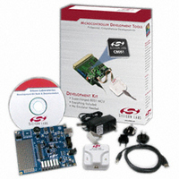
Manufacturer Part Number
C8051F530DK
Description
KIT DEV FOR C8051F520,F530
Manufacturer
Silicon Laboratories Inc
Type
Microcontrollerr
Specifications of C8051F530DK
Contents
Evaluation Board, Power Supply, USB Cables, Adapter and Documentation
Processor To Be Evaluated
C8051F52xA and C8051F53xA
Interface Type
USB
Lead Free Status / RoHS Status
Contains lead / RoHS non-compliant
For Use With/related Products
C8051F520, C8051F530
Lead Free Status / Rohs Status
Lead free / RoHS Compliant
Other names
336-1344


C8051F52x-53x-DK
8.3. Expansion I/O Connectors (J1, J2)
The two 24-pin Expansion I/O connectors J1 and J2 provide access to all signal pins of the C8051F530 devices.
Pins for V
area is also provided.
All I/O signals routed to connectors J1 and J2 are also routed to through-hole connection points between J1 and J2
and the prototyping area (see Figure 3 on page 8). Each connection point is labeled indicating the signal available
at the connection point. See Table 2 for a list of pin descriptions for J1 and J2.
8.4. Target Board DEBUG Interface (HDR1, HDR2)
The DEBUG connectors (HDR1 and HDR2) provide access to the DEBUG (C2) pins of the C8051F530 parts. They
are used to connect the USB Debug Adapter to the target board for in-circuit debugging and Flash programming.
Table 3 shows the DEBUG pin definitions.
10
Pin #
10
11
12
1
2
3
4
5
6
7
8
9
DD
Description
, GND, 5 V, Reset, Vbat, LIN, 3.3 V and Vrefin are also available. A small through-hole prototyping
P0.0_A
P0.1_A
P0.2_A
P0.3_A
P0.4_A
P0.5_A
P0.6_A
P0.7_A
P1.0_A
P1.1_A
P1.2_A
P1.3_A
J1
Pin #
13
14
15
16
17
18
19
20
21
22
23
24
Table 3. DEBUG Connector Pin Descriptions
Table 2. Pin Descriptions for J1 and J2
2, 3, 9
RST/C2CLK_A
Pin #
Description
10
1
4
5
6
7
8
V
P1.4_A
P1.5_A
P1.6_A
P1.7_A
DD
+3.3V
VBAT
GND
GND
+5V
LIN
of U1
+3 VD (+3.3 VDC)
Rev. 0.2
Not Connected
GND (Ground)
/RST (Reset)
Description
USB Power
C2CK
C2D
P3.0
Pin #
12
10
11
1
2
3
4
5
6
7
8
9
Description
P0.4_B
P0.5_B
P0.7_B
P1.0_B
P1.1_B
P1.2_B
P1.3_B
P0.0_B
P0.1_B
P0.2_B
P0.3_B
P0.6_B
J2
Pin #
13
14
15
16
17
18
19
20
21
22
23
24
RST/C2CLK_B
Description
V
VREFIN
P1.4_B
P1.5_B
P1.6_B
P1.7_B
DD
VBAT
GND
GND
+5V
LIN
of U2
Related parts for C8051F530DK
Image
Part Number
Description
Manufacturer
Datasheet
Request
R

Part Number:
Description:
SMD/C°/SINGLE-ENDED OUTPUT SILICON OSCILLATOR
Manufacturer:
Silicon Laboratories Inc
Part Number:
Description:
Manufacturer:
Silicon Laboratories Inc
Datasheet:
Part Number:
Description:
N/A N/A/SI4010 AES KEYFOB DEMO WITH LCD RX
Manufacturer:
Silicon Laboratories Inc
Datasheet:
Part Number:
Description:
N/A N/A/SI4010 SIMPLIFIED KEY FOB DEMO WITH LED RX
Manufacturer:
Silicon Laboratories Inc
Datasheet:
Part Number:
Description:
N/A/-40 TO 85 OC/EZLINK MODULE; F930/4432 HIGH BAND (REV E/B1)
Manufacturer:
Silicon Laboratories Inc
Part Number:
Description:
EZLink Module; F930/4432 Low Band (rev e/B1)
Manufacturer:
Silicon Laboratories Inc
Part Number:
Description:
I°/4460 10 DBM RADIO TEST CARD 434 MHZ
Manufacturer:
Silicon Laboratories Inc
Part Number:
Description:
I°/4461 14 DBM RADIO TEST CARD 868 MHZ
Manufacturer:
Silicon Laboratories Inc
Part Number:
Description:
I°/4463 20 DBM RFSWITCH RADIO TEST CARD 460 MHZ
Manufacturer:
Silicon Laboratories Inc
Part Number:
Description:
I°/4463 20 DBM RADIO TEST CARD 868 MHZ
Manufacturer:
Silicon Laboratories Inc
Part Number:
Description:
I°/4463 27 DBM RADIO TEST CARD 868 MHZ
Manufacturer:
Silicon Laboratories Inc
Part Number:
Description:
I°/4463 SKYWORKS 30 DBM RADIO TEST CARD 915 MHZ
Manufacturer:
Silicon Laboratories Inc
Part Number:
Description:
N/A N/A/-40 TO 85 OC/4463 RFMD 30 DBM RADIO TEST CARD 915 MHZ
Manufacturer:
Silicon Laboratories Inc
Part Number:
Description:
I°/4463 20 DBM RADIO TEST CARD 169 MHZ
Manufacturer:
Silicon Laboratories Inc