AQV252G Panasonic Electric Works, AQV252G Datasheet - Page 3
AQV252G
Manufacturer Part Number
AQV252G
Description
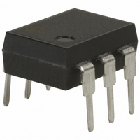
RELAY OPTO 60VAC/DC 2500MA 6-DIP
Manufacturer
Panasonic Electric Works
Series
PhotoMOS™ AQVr
Datasheets
1.OAC415-L.pdf
(3 pages)
2.OAC415-L.pdf
(6 pages)
3.AQV252GA.pdf
(3 pages)
4.AQV252G.pdf
(2 pages)
Specifications of AQV252G
Circuit
SPST-NO (1 Form A)
Output Type
AC, DC
On-state Resistance
120 mOhm
Load Current
2.5A
Voltage - Input
1.14VDC
Voltage - Load
0 ~ 60 V
Mounting Type
Through Hole
Termination Style
PC Pin
Package / Case
6-DIP (0.300", 7.62mm)
Capacitance
0.8 pF (Typ.)
Current, Rating
2.5 A
Dimensions
0.346 in. L x 0.252 in. W x 0.154 in. H
Function
General Purpose
Number Of Pins
6
Relay Type
Solid State
Resistance, On-state
0.08 Ω
Standards
VDE, CUL, UL
Temperature, Operating, Maximum
85 °C
Temperature, Operating, Minimum
-40 °C
Termination
Through Hole
Voltage, Control
60 V
Voltage, Rating
60 VAC/VDC
Lead Free Status / RoHS Status
Lead free / RoHS Compliant
Other names
255-1791
255-1791-5
255-1791
255-1791-5
255-1791
Available stocks
Company
Part Number
Manufacturer
Quantity
Price

Part Number:
AQV252G
Manufacturer:
NAIS
Quantity:
20 000
Part Number:
AQV252G2S
Manufacturer:
NAIS
Quantity:
20 000
Company:
Part Number:
AQV252GA
Manufacturer:
MURATA
Quantity:
2 000
Company:
Part Number:
AQV252GAX
Manufacturer:
OMRON
Quantity:
12 000
Company:
Part Number:
AQV252GAZ
Manufacturer:
Panasonic
Quantity:
12 000


Notes: 1. E
AQW21(SOP)
AQY41(SOP)
AQV41(SOP)
AQW21
AQW22
AQW25
AQW27
AQY41
AQV41
AQV45
Series
Series
Series
Type
2. Method of connecting the load at the output is divided into 3 types.
1
: Power source at input side; V
1
2
1
2
3
1
2
3
4
Terminal 3 cannot be
used, since it is in the in-
ternal circuit of the relay.
Schematic
8
7
6
5
4
3
6
5
4
IN
: Input voltage; I
configu-
All Rights Reserved © COPYRIGHT Matsushita Electric Works, Ltd.
Output
ration
2a
1b
1b
AC/DC
AC/DC
AC/DC
Load
DC
DC
F
: LED forward current; I
nection
Con-
—
—
A
B
C
Can be also connected as 2 Form B type. (However, the sum of the continuous load current
should not exceed the absolute maximum rating.)
(1) Two independent 1 Form A use
(2) 2 Form A use
E
E
E
E
E
E
E
E
1
1
1
1
1
1
1
1
IN
: Input current; V
I
I
F
I
I
F
I
I
F
F
I
I
F
F
F1
F2
1
2
3
4
1
2
3
4
1
2
1
2
3
1
2
3
1
2
3
1
2
3
L
: Load voltage; I
6
5
4
6
5
4
6
5
4
6
5
4
8
7
6
5
8
7
6
5
4
3
Load
Load
Load
Load
I
I
I
I
L1
L2
L1
L2
I
L
I
I
Load
Load
Load
Load
L
I
Load
L
L
Wiring diagram
I
L
L
: Load current; R: Current limit resistor.
V
V
V
V
+
–
–
+
L
L
L
+
–
L
(DC)
(DC)
(AC,DC)
(DC)
V
V
V
V
V
L1
L2
L1
L2
L
(AC,DC)
(AC,DC)
(AC,DC)
(AC,DC)
(AC,DC)
8
7
6
5
8
7
6
5
4
3
6
4
6
5
5
4
6
5
4
I
I
I
I
L1
L2
L1
L2
Load
Load
Load
Load
Load
Load
Load
Load
Load
I
I
I
L
L
L
I
I
L
L
V
V
V
V
L
+
–
–
+
V
V
V
V
L
L
+
–
L
V
(AC,DC)
(DC)
(DC)
L1
L2
L1
L2
(DC)
L
(AC,DC)
(AC,DC)
(AC,DC)
(AC,DC)
(AC,DC)
Related parts for AQV252G
Image
Part Number
Description
Manufacturer
Datasheet
Request
R

Part Number:
Description:
Solid State Relays Heat sink for AQ1 solid state relay
Manufacturer:
Panasonic
Datasheet:

Part Number:
Description:
SSR 2A 264VAC 5VDC-IN ZERO-CROSS
Manufacturer:
Panasonic Electric Works
Datasheet:

Part Number:
Description:
SSR 2A 264VAC 12VDC-INPUT
Manufacturer:
Panasonic Electric Works
Datasheet:

Part Number:
Description:
RELAY SSR ZC 0.9A 600V 8 DIP
Manufacturer:
Panasonic Electric Works
Datasheet:

Part Number:
Description:
RELAY SSR 1.2A 600V 8DIP
Manufacturer:
Panasonic Electric Works
Datasheet:
Part Number:
Description:
RELAY SSR ZC 1.2A 600VAC 8DIP
Manufacturer:
Panasonic Electric Works
Datasheet:
Part Number:
Description:
RELAY SSR ZC 0.6A 600V 8 DIP
Manufacturer:
Panasonic Electric Works
Datasheet:

Part Number:
Description:
RELAY SSR ZC 0.9A 600V 8 SMD
Manufacturer:
Panasonic Electric Works
Datasheet:
Part Number:
Description:
RELAY SSR NON-ZC 0.9A 600V 8 DIP
Manufacturer:
Panasonic Electric Works
Datasheet:

Part Number:
Description:
SSR ZC 30A 75-250VAC 4-6VDC
Manufacturer:
Panasonic Electric Works
Datasheet:

Part Number:
Description:
CONN SOCKET P4 .4MM 50POS SMD
Manufacturer:
Panasonic Electric Works
Datasheet:
Part Number:
Description:
CONN SOCKET .8MM 16POS SMD
Manufacturer:
Panasonic Electric Works
Datasheet:
Part Number:
Description:
CONN HEADER .8MM 16POS SMD
Manufacturer:
Panasonic Electric Works
Datasheet:
Part Number:
Description:
CONN SOCKET .8MM 20POS SMD
Manufacturer:
Panasonic Electric Works
Datasheet:
Part Number:
Description:
CONN SOCKET .8MM 20POS SMD
Manufacturer:
Panasonic Electric Works
Datasheet: