PVG612S-TPBF International Rectifier, PVG612S-TPBF Datasheet - Page 2
PVG612S-TPBF
Manufacturer Part Number
PVG612S-TPBF
Description
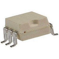
IC RELAY PHOTOVO 60V 1A 6-SMD
Manufacturer
International Rectifier
Series
PVG, HEXFET®r
Datasheet
1.PVG612S-TPBF.pdf
(5 pages)
Specifications of PVG612S-TPBF
Circuit
SPST-NO (1 Form A)
Output Type
AC, DC
On-state Resistance
500 mOhm
Load Current
1A
Voltage - Input
1.2VDC
Voltage - Load
0 ~ 60 V
Mounting Type
Surface Mount
Termination Style
Gull Wing
Package / Case
6-SMD (300 mil)
Input Type
DC
Output Voltage (max)
60V
Input Current (max)
25mA
Output Current
1000@Ta=40CmA
Isolation Voltage
4kV
Circuit Arrangement
1 Form A
Package Type
SMT
Output Device
MOSFET
Pin Count
6
Mounting
Surface Mount
Operating Temp Range
-40C to 85C
Operating Temperature Classification
Industrial
Rad Hardened
No
Load Voltage Max
60V
On State Resistance Max
500mohm
Contact Configuration
SPNO
Forward Current If
5mA
Relay Terminals
SMD
Load Current Rms Max
2A
Rohs Compliant
Yes
Leaded Process Compatible
Yes
Load Voltage Rating
60 V
Load Current Rating
2 A
Contact Form
1 Form A
Mounting Style
SMD/SMT
Maximum Operating Temperature
+ 85 C
Minimum Operating Temperature
- 40 C
Relay Type
AC/DC
Lead Free Status / RoHS Status
Lead free / RoHS Compliant
Available stocks
Company
Part Number
Manufacturer
Quantity
Price


Electrical Specifications (-40°C ≤ T
International Rectifier does not recommend the use of this product in aerospace, avionics, military or life support applications.
Users of this International Rectifier product in such applications assume all risks of such use and indemnify International
Rectifier against all damages resulting from such use.
Connection Diagrams
www.irf.com
INPUT CHARACTERISTICS
Minimum Control Current (see figure 1)
Maximum Control Current for Off-State Resistance @ T
Control Current Range (Caution: current limit input LED, see figure 6)
Maximum Reverse Voltage
OUTPUT CHARACTERISTICS
Operating Voltage Range
Maximum Load Current @ T
Maximum Pulsed Load Current @ T
Maximum On-State Resistance @T
Minimum Off-State Resistance @T
Maximum Turn-On Time @T
Maximum Turn-Off Time @T
Maximum Output Capacitance @ 50V
GENERAL CHARACTERISTICS
Minimum Dielectric Strength, Input-Output
Minimum Insulation Resistance, Input-Output, @T
Maximum Capacitance, Input-Output
Maximum Pin Soldering Temperature (10 seconds maximum)
Ambient Temperature Range:
For 1A pulsed load, 10mA Control (see figure 4)
For 500mA, 50 V
For 500mA, 50 V
DC
DC
load, 10mA Control
load, 10mA Control
A
A
A
= +40°C, 10mA Control (see figure 1)
=+25°C (see figure 7)
=+25°C (see figure 7)
A
A
A
=+25°C, ±48V (see figure 5)
=+25°C
DC
=+25°C (100 ms @ 10% Duty Cycle)
(see figure 2)
A
≤ +85°C unless otherwise specified)
A
=+25°C, 50%RH, 100V
A Connection
B Connection
C Connection
A Connection
A Connection
B Connection
C Connection
Operating
Storage
A
= +25°C
DC
-40 to +100
-40 to +85
5.0 to 25
Limits
Limits
0 to ±60
Limits
4000
+260
2.4A
10
500
250
150
130
10
5.0
0.4
6.0
1.0
1.5
2.0
2.0
0.5
1.0
12
8
Series PVG612PbF
V
(DC or AC peak)
A (AC or DC)
(AC or DC)
Units
Units
Units
A (DC)
A (DC)
V
mΩ
mΩ
mΩ
mA
mA
mA
ms
ms
RMS
pF
pF
°C
Ω
Ω
V
2
Related parts for PVG612S-TPBF
Image
Part Number
Description
Manufacturer
Datasheet
Request
R

Part Number:
Description:
SSR, PHOTO MOSFET, 60V, 2A
Manufacturer:
International Rectifier
Datasheet:

Part Number:
Description:
60v 1 Form A Photo Voltaic Relay In A 6-pin Smt Package
Manufacturer:
International Rectifier Corp.
Datasheet:
Part Number:
Description:
SCHOTTKY RECTIFIER
Manufacturer:
International Rectifier Corp.
Datasheet:
Part Number:
Description:
SCHOTTKY RECTIFIER
Manufacturer:
International Rectifier Corp.
Datasheet:
Part Number:
Description:
SCHOTTKY RECTIFIER
Manufacturer:
International Rectifier Corp.
Datasheet:
Part Number:
Description:
SCHOTTKY RECTIFIER
Manufacturer:
International Rectifier Corp.
Datasheet:
Part Number:
Description:
SCHOTTKY RECTIFIER
Manufacturer:
International Rectifier Corp.
Datasheet:
Part Number:
Description:
SCHOTTKY RECTIFIER
Manufacturer:
International Rectifier Corp.
Datasheet:
Part Number:
Description:
SCHOTTKY RECTIFIER
Manufacturer:
International Rectifier Corp.
Datasheet:
Part Number:
Description:
SCHOTTKY RECTIFIER
Manufacturer:
International Rectifier Corp.
Datasheet:
Part Number:
Description:
SCHOTTKY RECTIFIER
Manufacturer:
International Rectifier Corp.
Datasheet:
Part Number:
Description:
SCHOTTKY RECTIFIER
Manufacturer:
International Rectifier Corp.
Datasheet:
Part Number:
Description:
SCHOTTKY RECTIFIER
Manufacturer:
International Rectifier Corp.
Datasheet:
Part Number:
Description:
SCHOTTKY RECTIFIER
Manufacturer:
International Rectifier Corp.
Datasheet:
Part Number:
Description:
SCHOTTKY RECTIFIER
Manufacturer:
International Rectifier Corp.
Datasheet: