1N5913B ON Semiconductor, 1N5913B Datasheet

DIODE ZENER 3W 3.3V DO-41

1N5913B

Manufacturer Part Number
1N5913B
Description
DIODE ZENER 3W 3.3V DO-41
Manufacturer
ON Semiconductor
Series
Surmetic™r
Datasheet

Specifications of 1N5913B

Voltage - Zener (nom) (vz)
3.3V
Voltage - Forward (vf) (max) @ If
1.5V @ 200mA
Current - Reverse Leakage @ Vr
100µA @ 1V
Tolerance
±5%
Power - Max
3W
Impedance (max) (zzt)
10 Ohm
Mounting Type
Through Hole
Package / Case
DO-204AL, DO-41, Axial
Operating Temperature
-65°C ~ 200°C
Lead Free Status / RoHS Status
Contains lead / RoHS non-compliant

Available stocks

Company
Part Number
Manufacturer
Quantity
Price
Part Number:
1N5913B
Manufacturer:
ST
0
1N5913B Series
3 W DO−41 Surmetict 30
Zener Voltage Regulators
excellent operating characteristics that reflect the superior capabilities
of silicon−oxide passivated junctions. All this in an axial−lead,
transfer−molded plastic package that offers protection in all common
environmental conditions.
Features
Mechanical Characteristics
CASE:
FINISH:
readily solderable
MAXIMUM LEAD TEMPERATURE FOR SOLDERING PURPOSES:
260°C, 1/16″ from the case for 10 seconds
POLARITY:
MOUNTING POSITION:
Maximum ratings are those values beyond which device damage can occur.
Maximum ratings applied to the device are individual stress limit values (not
normal operating conditions) and are not valid simultaneously. If these limits are
exceeded, device functional operation is not implied, damage may occur and
reliability may be affected.
*For additional information on our Pb−Free strategy and soldering details, please
MAXIMUM RATINGS
© Semiconductor Components Industries, LLC, 2006
April, 2006 − Rev. 5
Max. Steady State Power Dissipation
Steady State Power Dissipation
Operating and Storage
download the ON Semiconductor Soldering and Mounting Techniques
Reference Manual, SOLDERRM/D.
This is a complete series of 3 W Zener diodes with limits and
Zener Voltage Range − 3.3 V to 200 V
ESD Rating of Class 3 (>16 KV) per Human Body Model
Surge Rating of 98 W @ 1 ms
Maximum Limits Guaranteed on up to Six Electrical Parameters
Package No Larger than the Conventional 1 W Package
Pb−Free Packages are Available
@ T
Derate above 75°C
@ T
Derate above 50°C
Temperature Range
A
L
Void free, transfer−molded, thermosetting plastic
= 75°C, Lead Length = 3/8″
= 50°C
All external surfaces are corrosion resistant and leads are
Cathode indicated by polarity band
Rating
Any
Symbol
T
J
P
P
, T
D
D
stg
−65 to
Value
+200
6.67
24
3
1
1
mW/°C
mW/°C
Unit
°C
W
W
†For information on tape and reel specifications,
1N59xxB, G
1N59xxBRL, G
including part orientation and tape sizes, please
refer to our Tape and Reel Packaging Specification
Brochure, BRD8011/D.
Device
Cathode
A
1N59xxB = Device Number
YY
WW
G
(Note: Microdot may be in either location)
ORDERING INFORMATION
MARKING DIAGRAM
http://onsemi.com
Axial Lead
Axial Lead
= Assembly Location
= Year
= Work Week
= Pb−Free Package
(Pb−Free)
(Pb−Free)
Package
YYWWG
59xxB
1N
Publication Order Number:
A
G
AXIAL LEAD
PLASTIC
CASE 59
STYLE 1
6000/Tape & Reel
2000 Units/Box
Anode
Shipping
1N5913B/D

Related parts for 1N5913B

1N5913B Summary of contents

Page 1

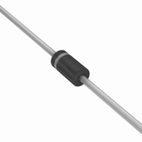
... Series 3 W DO−41 Surmetict 30 Zener Voltage Regulators This is a complete series Zener diodes with limits and excellent operating characteristics that reflect the superior capabilities of silicon−oxide passivated junctions. All this in an axial−lead, transfer−molded plastic package that offers protection in all common environmental conditions ...

Page 2

... F F Symbol Parameter V Reverse Zener Voltage @ Reverse Current ZT Z Maximum Zener Impedance @ Reverse Current ZK Z Maximum Zener Impedance @ Reverse Leakage Current @ Breakdown Voltage R I Forward Current F V Forward Voltage @ Maximum DC Zener Current ZM 1N5913B Series http://onsemi.com Zener Voltage Regulator V ...

Page 3

... ELECTRICAL CHARACTERISTICS (T Zener Voltage (Note 2) † Device Device Min (Note 1) Marking 1N5913B, G 1N5913B 3.14 1N5917B, G 1N5917B 4.47 1N5919B, G 1N5919B 5.32 1N5920B, G 1N5920B 5.89 1N5921B, G 1N5921B 6.46 1N5923B, G 1N5923B 7.79 1N5924B, G 1N5924B 8.65 1N5925B, G 1N5925B 9.50 1N5926B, G 1N5926B 10.45 1N5927B, G 1N5927B 11.40 ...

Page 4

... PW, PULSE WIDTH (ms) Figure 3. Maximum Surge Power 1N5913B Series L = LEAD LENGTH TO HEAT SINK L = 1/8″ 3/8″ 100 120 140 160 T , LEAD TEMPERATURE (°C) L NOTE: BELOW 0.1 SECOND, THERMAL RESPONSE CURVE IS APPLICABLE TO ANY LEAD LENGTH (L). ...

Page 5

... Using the measured value the junction temperature L may be determined by 1N5913B Series DT is the increase in junction temperature above the lead JL temperature and may be found from Figure 2 for a train of power pulses (L = 3/8 inch) or from Figure 10 for dc power. For worst-case design, using expected limits and the extremes ...

Page 6

... V , ZENER VOLTAGE (VOLTS) Z Figure 3.3 thru 10 Volts 0.5 0.2 0.1 100 150 200 250 300 V , ZENER VOLTAGE (VOLTS) Z Figure 100 thru 400 Volts Z 1N5913B Series 1000 500 200 100 (VOLTS) (Figures 7, 8 and 9) 100 0.5 0.3 0.2 0 ...

Page 7

... Series PACKAGE DIMENSIONS AXIAL LEAD CASE 59−10 ISSUE POLARITY INDICATOR OPTIONAL AS NEEDED F (SEE STYLES) K http://onsemi.com NOTES: 1. DIMENSIONING AND TOLERANCING PER ANSI Y14.5M, 1982. 2. CONTROLLING DIMENSION: INCH. 3. ALL RULES AND NOTES ASSOCIATED WITH JEDEC DO−41 OUTLINE SHALL APPLY 4. POLARITY DENOTED BY CATHODE BAND. ...

Page 8

... P.O. Box 61312, Phoenix, Arizona 85082−1312 USA Phone: 480−829−7710 or 800−344−3860 Toll Free USA/Canada Fax: 480−829−7709 or 800−344−3867 Toll Free USA/Canada Email: orderlit@onsemi.com 1N5913B Series N. American Technical Support: 800−282−9855 Toll Free USA/Canada Japan: ON Semiconductor, Japan Customer Focus Center 2− ...

Related keywords