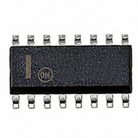
NE5517D ON Semiconductor, NE5517D Datasheet

NE5517D
Specifications of NE5517D
Available stocks
Related parts for NE5517D
NE5517D Summary of contents
Page 1
... Dolby® HX Systems • Current-Controlled Amplifiers, Filters • Current-Controlled Oscillators, Impedances *For additional information on our Pb−Free strategy and soldering details, please download the ON Semiconductor Soldering and Mounting Techniques Reference Manual, SOLDERRM/D. © Semiconductor Components Industries, LLC, 2006 April, 2006 − Rev hence eliminating ...
Page 2
PIN DESCRIPTION Pin No. Symbol 1 I ABCa + − V− BUFFERa 8 VO BUFFERa 9 VO BUFFERb 10 IN BUFFERb ...
Page 3
... V+ of output buffers and amplifiers are internally connected. MAXIMUM RATINGS Rating Supply Voltage (Note °C (Still Air) (Note 2) Power Dissipation, T amb NE5517N, NE5517AN NE5517D, AU5517D Thermal Resistance, Junction−to−Ambient D Package N Package Differential Input Voltage Diode Bias Current Amplifier Bias Current Output Short-Circuit Duration ...
Page 4
ELECTRICAL CHARACTERISTICS Test Conditions Characteristic Input Offset Voltage Overtemperature Range DV /DT Avg Input Offset Voltage OS V Including Diodes Diode Bias Current OS (I 5.0 mA ≤ I Input Offset Change Input Offset Current DI /DT Avg. ...
Page 5
TYPICAL PERFORMANCE CHARACTERISTICS ±15V +125°C 1 -55° +25°C +125° 0.1mA 1mA 10mA 100mA 1000mA AMPLIFIER BIAS CURRENT (I ) ABC Figure 3. Input Offset ...
Page 6
TYPICAL PERFORMANCE CHARACTERISTICS 2000 1800 -55°C 1600 1400 +25°C 1200 1000 +125°C 800 600 400 200 0 0.1mA 1mA 10mA 100mA 1000mA AMPLIFIER BIAS CURRENT (I ) ABC Figure 12. Amplifier Bias Voltage vs. Amplifier Bias Current ...
Page 7
INPUT 51W CIRCUIT DESCRIPTION The circuit schematic diagram of one-half of the AU5517/NE5517, a dual operational transconductance amplifier with linearizing diodes and impedance buffers, is shown in Figure 21. Transconductance Amplifier The transistor pair, Q and Q , forms ...
Page 8
Linearizing Diodes For V greater than a few millivolts, Equation 3 becomes IN invalid and the transconductance increases non-linearly. Figure 22 shows how the internal diodes can linearize the transfer function of the operational amplifier. Assume D and D are ...
Page 9
Stereo Amplifier With Gain Control Figure 24 shows a stereo amplifier with variable gain via a control input. Excellent tracking of typical 0 easy to achieve. With the potentiometer, R adjusted. For AC-coupled amplifiers, the potentiometer may be ...
Page 10
Voltage-Controlled Resistor (VCR) Because an OTA is capable of producing an output current proportional to the input voltage, a voltage variable resistor can be made. Figure 26 shows how this is done. A voltage presented at the R terminals forces ...
Page 11
V IN 200W NOTE g(R ) RA) 2pC O Figure 28. Voltage-Controlled Low-Pass Filter +V CC 100kW V OS NULL -V CC 1kW NOTE g(R ) RA) ...
Page 12
CC 10kW NE5517/A − 6 1kW −V CC 30kW − NE5517 −V CC Figure 32. Triangle−Square Wave Generator (VCO 470kW 1 V ...
Page 13
... ORDERING INFORMATION Device AU5517DR2 AU5517DR2G NE5517D NE5517DG NE5517DR2 NE5517DR2G NE5517N NE5517NG NE5517AN NE5517ANG †For information on tape and reel specifications, including part orientation and tape sizes, please refer to our Tape and Reel Packaging Specifications Brochure, BRD8011/D. NE5517, NE5517A, AU5517 Temperature Range Package SOIC− ...
Page 14
... American Technical Support: 800−282−9855 Toll Free USA/Canada Japan: ON Semiconductor, Japan Customer Focus Center 2−9−1 Kamimeguro, Meguro−ku, Tokyo, Japan 153−0051 Phone: 81−3−5773−3850 http://onsemi.com 14 NOTES: 1. DIMENSIONING AND TOLERANCING PER ANSI Y14.5M, 1982. 2. CONTROLLING DIMENSION: MILLIMETER. ...


