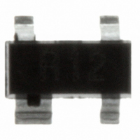
SR12.TCT Semtech, SR12.TCT Datasheet - Page 5

SR12.TCT
Manufacturer Part Number
SR12.TCT
Description
IC TVS ARRAY 2-LINE 12V SOT-143
Manufacturer
Semtech
Series
RailClamp®r
Datasheet
1.SR12.TCT.pdf
(8 pages)
Specifications of SR12.TCT
Voltage - Reverse Standoff (typ)
12V
Voltage - Breakdown
13.3V
Power (watts)
500W
Polarization
2 Channel Array - Unidirectional
Mounting Type
Surface Mount
Package / Case
SOT-143, SOT-143B, TO-253AA
Lead Free Status / RoHS Status
Lead free / RoHS Compliant
Other names
SR12TR
Available stocks
Company
Part Number
Manufacturer
Quantity
Price
Part Number:
SR12.TCT
Manufacturer:
SEMTECH/美国升特
Quantity:
20 000
For negative events, the bottom diode will be biased
when the voltage exceeds the V
approximation, the clamping voltage due to the charac-
teristics of the protection diodes is given by:
PIN Descriptions
V
V
However, for fast rise time transient events, the
effects of parasitic inductance must also be consid-
ered as shown in Figure 2. Therefore, the actual
clamping voltage seen by the protected circuit will be:
V
V
ESD current reaches a peak amplitude of 30A in 1ns
for a level 4 ESD contact discharge per IEC 1000-4-2.
Therefore, the voltage overshoot due to 1nH of series
inductance is:
V = L
Example:
Consider a V
steering diode and a series trace inductance of 10nH.
The clamping voltage seen by the protected IC for a
positive 8kV (30A) ESD pulse will be:
V
This does not take into account that the ESD current is
directed into the supply rail, potentially damaging any
components that are attached to that rail. Also note
that it is not uncommon for the V
exceed the damage threshold of the protected IC. This
is due to the relatively small junction area of typical
discrete components. It is also possible that the
power dissipation capability of the discrete diode will
be exceeded, thus destroying the device.
The RailClamp is designed to overcome the inherent
disadvantages of using discrete signal diodes for ESD
suppression. The RailClamp’s integrated TVS diode
helps to mitigate the effects of parasitic inductance in
PROTECTION PRODUCTS
Applications Information (continued)
C
C
C
C
C
2005 Semtech Corp.
= V
= -V
= V
= -V
= 5V + 30V + (10nH X 30V/nH) = 335V
P
CC
CC
F
di
F
- L
+ V
+ V
ESD
G
/dt = 1X10
F
F
di
CC
+ L
ESD
= 5V, a typical V
(for positive duration pulses)
(for negative duration pulses)
P
/dt
di
ESD
/dt (for positive duration pulses)
-9
(30 / 1X10
(for negative duration pulses)
F
F
of 30V (at 30A) for the
of the diode. At first
F
of discrete diodes to
-9
) = 30V
5
When Using Discrete Components to Implement
When Using Discrete Components to Implement
When Using Discrete Components to Implement
When Using Discrete Components to Implement
When Using Discrete Components to Implement
Figure 2 - The Effects of Parasitic Inductance
Figure 2 - The Effects of Parasitic Inductance
Figure 2 - The Effects of Parasitic Inductance
Figure 2 - The Effects of Parasitic Inductance
Figure 2 - The Effects of Parasitic Inductance
Figure 1 - “Rail-
Figure 1 - “Rail-
Figure 1 - “Rail-
Figure 1 - “Rail-
Figure 1 - “Rail-T T T T T o-Rail” Pr
Figure 3 - Rail-
Figure 3 - Rail-
Figure 3 - Rail-T T T T T o-Rail Pr
Figure 3 - Rail-
Figure 3 - Rail-
Rail-
Rail-
Rail-
Rail-
Rail-T T T T T o-Rail Pr
RailClam
RailClam
RailClam
RailClam
RailClamp T
(First Approximation)
(First Approximation)
(First Approximation)
(First Approximation)
(First Approximation)
o-Rail Pr
o-Rail Pr
o-Rail Pr
o-Rail Pro o o o o t t t t t ection
o-Rail” Pr
o-Rail” Pr
o-Rail” Pr
o-Rail” Pro o o o o t t t t t ection T
o-Rail Pr
o-Rail Pr
o-Rail Pro o o o o t t t t t ection Using
o-Rail Pr
p T
p T V V V V V S Arra
p T
p T
S Arra
S Arra
S Arrays ys ys ys ys
S Arra
ection
ection
ection
ection
ection T
ection T
ection T
ection Topology
ection Using
ection Using
ection Using
ection Using
www.semtech.com
opology
opology
opology
opology
SR12


