NUP4201MR6T1G ON Semiconductor, NUP4201MR6T1G Datasheet
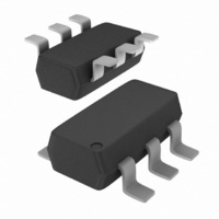
IC TVS DIODE ARRAY HS LINE 6TSOP

NUP4201MR6T1G

Manufacturer Part Number
NUP4201MR6T1G
Description
IC TVS DIODE ARRAY HS LINE 6TSOP
Manufacturer
ON Semiconductor
Datasheet

Specifications of NUP4201MR6T1G

Voltage - Reverse Standoff (typ)
5V
Voltage - Breakdown
6V
Power (watts)
500W
Polarization
4 Channel Array - Bidirectional
Mounting Type
Surface Mount
Package / Case
SC-74-6
Polarity
Unidirectional
Clamping Voltage
20 V
Operating Voltage
5 V
Breakdown Voltage
6 V
Termination Style
SMD/SMT
Peak Surge Current
25 A
Peak Pulse Power Dissipation
500 W
Capacitance
5 pF
Maximum Operating Temperature
+ 125 C
Minimum Operating Temperature
- 40 C
Dimensions
1.5 mm W x 3 mm L
Lead Free Status / RoHS Status
Lead free / RoHS Compliant
Other names
NUP4201MR6T1GOSTR

Available stocks

Company
Part Number
Manufacturer
Quantity
Price
Part Number:
NUP4201MR6T1G
Manufacturer:
ON
Quantity:
2 000
Part Number:
NUP4201MR6T1G
Manufacturer:
ON
Quantity:
30 000
Part Number:
NUP4201MR6T1G
Manufacturer:
ONSEMI
Quantity:
1 339
Part Number:
NUP4201MR6T1G
Manufacturer:
ON
Quantity:
2 846
Part Number:
NUP4201MR6T1G
Manufacturer:
ON
Quantity:
8 000
Part Number:
NUP4201MR6T1G
Manufacturer:
ON/安森美
Quantity:
20 000
Part Number:
NUP4201MR6T1G
Manufacturer:
ON
Quantity:
5 444
Company:
Part Number:
NUP4201MR6T1G
Quantity:
9 000
NUP4201MR6
Transient Voltage
Suppressors
ESD Protection Diodes with Low
Clamping Voltage
protect high speed data lines from ESD, EFT, and lighting.
Features
Typical Applications
Stresses exceeding Maximum Ratings may damage the device. Maximum
Ratings are stress ratings only. Functional operation above the Recommended
Operating Conditions is not implied. Extended exposure to stresses above the
Recommended Operating Conditions may affect device reliability.
1. Non−repetitive current pulse per Figure 5 (Pin 5 to Pin 2)
See Application Note AND8308/D for further description of
survivability specs.
MAXIMUM RATINGS
© Semiconductor Components Industries, LLC, 2009
September, 2009 − Rev. 5
Peak Power Dissipation
8 x 20 mS @ T
Operating Junction Temperature Range
Storage Temperature Range
Lead Solder Temperature −
Maximum (10 Seconds)
Human Body Model (HBM)
Machine Model (MM)
IEC 61000−4−2 Air (ESD)
IEC 61000−4−2 Contact (ESD)
IEC 61000−4−4 (5/50 ns)
The NUP4201MR6 transient voltage suppressor is designed to
SOT−23 6 Lead
IEC 61000−4−2 Level 4 ESD Protection
Low Clamping Voltage
Stand−Off Voltage: 5 V
Low Leakage
TSOP−6 is footprint compatible with SC−74, SC−59 6 Lead and
Protection for the Following IEC Standards:
UL Flammability Rating of 94 V−0
Pb−Free Package is Available
High Speed Communication Line Protection
USB 1.1 and 2.0 Power and Data Line Protection
Digital Video Interface (DVI)
Monitors and Flat Panel Displays
NUP4201MR6T1
NUP4201MR6T1G
A
= 25°C (Note 1)
Rating
(T
J
= 25°C unless otherwise noted)
Symbol
ESD
EFT
T
P
T
T
stg
pk
J
L
−40 to +125
−55 to +150
16000
20000
20000
Value
500
235
260
400
40
1
Unit
°C
°C
°C
°C
W
V
A
†For information on tape and reel specifications,
NUP4201MR6T1
NUP4201MR6T1G
including part orientation and tape sizes, please
refer to our Tape and Reel Packaging Specification
Brochure, BRD8011/D.
TSOP−6 LOW CAPACITANCE
500 WATTS PEAK POWER
63 = Specific Device Code
M = Date Code
G = Pb−Free Package
(Note: Microdot may be in either location)
*Date Code orientation may vary
Device
depending upon manufacturing location.
I/O 1
I/O 3
V
ORDERING INFORMATION
DIODE TVS ARRAY
N
2
PIN CONFIGURATION
MARKING DIAGRAM
http://onsemi.com
AND SCHEMATIC
6 VOLTS
CASE 318G
6
PLASTIC
TSOP−6
(Pb−Free)
Package
TSOP−6
TSOP−6
63
Publication Order Number:
G
1
G
3000/Tape & Reel
3000/Tape & Reel
NUP4201MR6/D
6 I/O
5 V
4 I/O
Shipping
P

Related parts for NUP4201MR6T1G

NUP4201MR6T1G Summary of contents

Page 1

... T L 235 °C 260 °C ESD 16000 V 400 20000 20000 EFT 40 A NUP4201MR6T1 NUP4201MR6T1G †For information on tape and reel specifications, 1 http://onsemi.com TSOP−6 LOW CAPACITANCE DIODE TVS ARRAY 500 WATTS PEAK POWER 6 VOLTS PIN CONFIGURATION AND SCHEMATIC I I I/O 3 ...

Page 2

ELECTRICAL CHARACTERISTICS (T = 25°C unless otherwise noted) A Symbol Parameter I Maximum Reverse Peak Pulse Current PP V Clamping Voltage @ Working Peak Reverse Voltage RWM I Maximum Reverse Leakage Current @ ...

Page 3

... ON Semiconductor has developed a way to examine the entire voltage waveform across the ESD protection diode over the time domain of an ESD pulse in the form of an oscilloscope screenshot, which can be found on the datasheets for all ESD protection diodes ...

Page 4

TYPICAL PERFORMANCE CURVES 100 5.0 4.5 4.0 3.5 3.0 I/O−Ground 2.5 2.0 I/O lines 1.5 1.0 0.5 0 REVERSE VOLTAGE (V) BR Figure ...

Page 5

The new NUP4201MR6 is a low capacitance TVS diode array designed to protect sensitive electronics such as communications systems, computers, and computer peripherals against damage due to ESD events or transient overvoltage conditions. Because of its low capacitance, it can ...

Page 6

... ESD transient current levels. This voltage combined −VF with the smaller die can result in device failure. The ON Semiconductor NUP4201MR6 was developed to overcome the disadvantages encountered when using discrete diodes for ESD protection. This device integrates a TVS diode within a network of steering diodes. ...

Page 7

UPSTREAM USB PORT V BUS V BUS D+ D− V BUS Controller GND NUP2201DT1 Figure 10. ESD Protection for USB Port TX+ TX− PHY Ethernet RX+ (10/100) RX− GND Figure 11. Protection for Ethernet 10/100 (Differential mode) TYPICAL ...

Page 8

RTIP RRING V CC T1/E1 TRANCEIVER TTIP TRING Figure 12. TI/E1 Interface Protection http://onsemi.com NUP4201MR6 ...

Page 9

... ON Semiconductor Soldering and Mounting Techniques Reference Manual, SOLDERRM/D. N. American Technical Support: 800−282−9855 Toll Free USA/Canada Europe, Middle East and Africa Technical Support: Phone: 421 33 790 2910 Japan Customer Focus Center Phone: 81− ...

Related keywords