PIC18F13K50-I/MQ Microchip Technology, PIC18F13K50-I/MQ Datasheet - Page 148
PIC18F13K50-I/MQ
Manufacturer Part Number
PIC18F13K50-I/MQ
Description
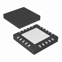
IC PIC MCU FLASH 512KX8 20-QFN
Manufacturer
Microchip Technology
Series
PIC® XLP™ 18Fr
Datasheets
1.PIC18F13K50-ISS.pdf
(420 pages)
2.PIC18F13K50-ISS.pdf
(40 pages)
3.PIC18F13K50-ISS.pdf
(10 pages)
4.PIC18F13K50-ISS.pdf
(2 pages)
5.PIC18F14K50-IP.pdf
(422 pages)
Specifications of PIC18F13K50-I/MQ
Program Memory Type
FLASH
Program Memory Size
8KB (4K x 16)
Package / Case
20-QFN
Core Processor
PIC
Core Size
8-Bit
Speed
48MHz
Connectivity
I²C, SPI, UART/USART, USB
Peripherals
Brown-out Detect/Reset, POR, PWM, WDT
Number Of I /o
14
Eeprom Size
256 x 8
Ram Size
512 x 8
Voltage - Supply (vcc/vdd)
1.8 V ~ 5.5 V
Data Converters
A/D 11x10b
Oscillator Type
Internal
Operating Temperature
-40°C ~ 85°C
Processor Series
PIC18F
Core
PIC
Data Bus Width
8 bit
Data Ram Size
512 B
Interface Type
EUSART/I2C/MSSP/SPI/USB
Maximum Clock Frequency
48 MHz
Number Of Programmable I/os
15
Number Of Timers
4
Operating Supply Voltage
1.8 V to 5.6 V
Maximum Operating Temperature
+ 85 C
Mounting Style
SMD/SMT
3rd Party Development Tools
52715-96, 52716-328, 52717-734, 52712-325, EWPIC18
Development Tools By Supplier
PG164130, DV164035, DV244005, DV164005, DM164127, DV164126
Minimum Operating Temperature
- 40 C
On-chip Adc
11-ch x 10-bit
Lead Free Status / RoHS Status
Lead free / RoHS Compliant
For Use With
DV164126 - KIT DEVELOPMENT USB W/PICKIT 2DM164127 - KIT DEVELOPMENT USB 18F14/13K50
Lead Free Status / Rohs Status
Lead free / RoHS Compliant
Available stocks
Company
Part Number
Manufacturer
Quantity
Price

Part Number:
PIC18F13K50-I/MQ
Manufacturer:
MICROCHIP/微芯
Quantity:
20 000


PIC18F/LF1XK50
15.3
The MSSP module in I
master and slave functions (including general call
support) and provides interrupts on Start and Stop bits
in hardware to determine a free bus (multi-master
function). The MSSP module implements the standard
mode specifications as well as 7-bit and 10-bit
addressing.
Two pins are used for data transfer:
• Serial clock – SCL
• Serial data – SDA
FIGURE 15-7:
DS41350E-page 148
Note:
SDI/SDA
SCK/SCL
I
2
C Mode
The user must configure these pins as
inputs with the corresponding TRIS bits.
Read
Shift
Clock
MSb
MSSP BLOCK DIAGRAM
(I
2
2
SSPMSK Reg
SSPADD Reg
Match Detect
C mode fully implements all
Stop bit Detect
C™ MODE)
SSPBUF Reg
SSPSR Reg
Start and
LSb
Write
(SSPSTAT Reg)
Internal
Data Bus
Addr Match
Set, Reset
S, P bits
Preliminary
15.3.1
The MSSP module has seven registers for I
operation. These are:
• MSSP Control Register 1 (SSPCON1)
• MSSP Control Register 2 (SSPCON2)
• MSSP Status register (SSPSTAT)
• Serial Receive/Transmit Buffer Register
• MSSP Shift Register (SSPSR) – Not directly
• MSSP Address Register (SSPADD)
• MSSP Address Mask (SSPMSK)
SSPCON1, SSPCON2 and SSPSTAT are the control
and STATUS registers in I
SSPCON1 and SSPCON2 registers are readable and
writable. The lower 6 bits of the SSPSTAT are read-only.
The upper two bits of the SSPSTAT are read/write.
SSPSR is the shift register used for shifting data in or
out. SSPBUF is the buffer register to which data bytes
are written to or read from.
When the MSSP is configured in Master mode, the
SSPADD register acts as the Baud Rate Generator
reload value. When the MSSP is configured for I
slave mode the SSPADD register holds the slave
device address. The MSSP can be configured to
respond to a range of addresses by qualifying selected
bits of the address register with the SSPMSK register.
In receive operations, SSPSR and SSPBUF together
create a double-buffered receiver. When SSPSR
receives a complete byte, it is transferred to SSPBUF
and the SSPIF interrupt is set.
During
double-buffered. A write to SSPBUF will write to both
SSPBUF and SSPSR.
(SSPBUF)
accessible
transmission,
REGISTERS
2010 Microchip Technology Inc.
the
2
C mode operation. The
SSPBUF
is
not
2
2
C
C
Related parts for PIC18F13K50-I/MQ
Image
Part Number
Description
Manufacturer
Datasheet
Request
R

Part Number:
Description:
Manufacturer:
Microchip Technology Inc.
Datasheet:
Part Number:
Description:
Manufacturer:
Microchip Technology Inc.
Datasheet:
Part Number:
Description:
Manufacturer:
Microchip Technology Inc.
Datasheet:
Part Number:
Description:
Manufacturer:
Microchip Technology Inc.
Datasheet:
Part Number:
Description:
Manufacturer:
Microchip Technology Inc.
Datasheet:
Part Number:
Description:
Manufacturer:
Microchip Technology Inc.
Datasheet:
Part Number:
Description:
Manufacturer:
Microchip Technology Inc.
Datasheet:
Part Number:
Description:
Manufacturer:
Microchip Technology Inc.
Datasheet: