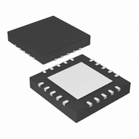
PIC18F14K50-I/MQ Microchip Technology, PIC18F14K50-I/MQ Datasheet - Page 118

PIC18F14K50-I/MQ
Manufacturer Part Number
PIC18F14K50-I/MQ
Description
IC PIC MCU FLASH 768KX16 20-QFN
Manufacturer
Microchip Technology
Series
PIC® XLP™ 18Fr
Datasheets
1.PIC18F13K50-ISS.pdf
(420 pages)
2.PIC18F13K50-ISS.pdf
(10 pages)
3.PIC18F13K50-ISS.pdf
(2 pages)
4.PIC18F14K50-ISS.pdf
(4 pages)
5.PIC18F14K50-IP.pdf
(422 pages)
Specifications of PIC18F14K50-I/MQ
Program Memory Type
FLASH
Program Memory Size
16KB (8K x 16)
Package / Case
20-QFN
Core Processor
PIC
Core Size
8-Bit
Speed
48MHz
Connectivity
I²C, SPI, UART/USART, USB
Peripherals
Brown-out Detect/Reset, POR, PWM, WDT
Number Of I /o
14
Eeprom Size
256 x 8
Ram Size
768 x 8
Voltage - Supply (vcc/vdd)
1.8 V ~ 5.5 V
Data Converters
A/D 11x10b
Oscillator Type
Internal
Operating Temperature
-40°C ~ 85°C
Processor Series
PIC18F
Core
PIC
Data Bus Width
8 bit
Data Ram Size
768 B
Interface Type
EUSART/I2C/MSSP/SPI/USB
Maximum Clock Frequency
48 MHz
Number Of Programmable I/os
15
Number Of Timers
4
Operating Supply Voltage
1.8 V to 5.6 V
Maximum Operating Temperature
+ 85 C
Mounting Style
SMD/SMT
3rd Party Development Tools
52715-96, 52716-328, 52717-734, 52712-325, EWPIC18
Development Tools By Supplier
PG164130, DV164035, DV244005, DV164005
Minimum Operating Temperature
- 40 C
On-chip Adc
11-ch x 10-bit
Package
20QFN EP
Device Core
PIC
Family Name
PIC18
Maximum Speed
48 MHz
Lead Free Status / RoHS Status
Lead free / RoHS Compliant
For Use With
DV164126 - KIT DEVELOPMENT USB W/PICKIT 2DM164127 - KIT DEVELOPMENT USB 18F14/13K50
Lead Free Status / Rohs Status
Lead free / RoHS Compliant
- PIC18F13K50-ISS PDF datasheet
- PIC18F13K50-ISS PDF datasheet #2
- PIC18F13K50-ISS PDF datasheet #3
- PIC18F14K50-ISS PDF datasheet #4
- PIC18F14K50-IP PDF datasheet #5
- Current page: 118 of 420
- Download datasheet (4Mb)
PIC18F/LF1XK50
In addition to the expanded range of modes available
through the CCP1CON register and ECCP1AS
register, the ECCP module has two additional registers
associated with Enhanced PWM operation and
auto-shutdown features. They are:
• PWM1CON (Dead-band delay)
• PSTRCON (output steering)
14.1
The enhanced CCP module may have up to four PWM
outputs, depending on the selected operating mode.
These outputs, designated P1A through P1D, are
multiplexed with I/O pins on PORTC. The outputs that
are active depend on the CCP operating mode
selected. The pin assignments are summarized in
Table
To configure the I/O pins as PWM outputs, the proper
PWM mode must be selected by setting the P1M<1:0>
and CCP1M<3:0> bits. The appropriate TRISC
direction bits for the port pins must also be set as
outputs.
14.1.1
The CCP modules utilize Timers 1, 2 or 3, depending
on the mode selected. Timer1 and Timer3 are available
to modules in Capture or Compare modes, while
Timer2 is available for modules in PWM mode.
TABLE 14-1:
The assignment of a particular timer to a module is
determined by the Timer-to-CCP enable bits in the
T3CON register
between
Figure
capture operation will not work reliably.
DS41350E-page 118
CCP/ECCP Mode
14-2.
14-1. In Asynchronous Counter mode, the
Compare
Capture
ECCP Outputs and Configuration
PWM
the two modules are
CCP MODULE AND TIMER
RESOURCES
CCP MODE – TIMER
RESOURCE
(Register
13-1). The interactions
Timer1 or Timer3
Timer1 or Timer3
Timer Resource
Timer2
summarized in
Preliminary
2010 Microchip Technology Inc.
Related parts for PIC18F14K50-I/MQ
Image
Part Number
Description
Manufacturer
Datasheet
Request
R

Part Number:
Description:
Manufacturer:
Microchip Technology Inc.
Datasheet:

Part Number:
Description:
Manufacturer:
Microchip Technology Inc.
Datasheet:

Part Number:
Description:
Manufacturer:
Microchip Technology Inc.
Datasheet:

Part Number:
Description:
Manufacturer:
Microchip Technology Inc.
Datasheet:

Part Number:
Description:
Manufacturer:
Microchip Technology Inc.
Datasheet:

Part Number:
Description:
Manufacturer:
Microchip Technology Inc.
Datasheet:

Part Number:
Description:
Manufacturer:
Microchip Technology Inc.
Datasheet:

Part Number:
Description:
Manufacturer:
Microchip Technology Inc.
Datasheet:


