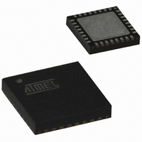
ATTINY28V-1MU Atmel, ATTINY28V-1MU Datasheet - Page 3

ATTINY28V-1MU
Manufacturer Part Number
ATTINY28V-1MU
Description
IC MCU AVR 2K 1.8V 1.2MHZ 32-QFN
Manufacturer
Atmel
Series
AVR® ATtinyr
Specifications of ATTINY28V-1MU
Core Processor
AVR
Core Size
8-Bit
Speed
1.2MHz
Peripherals
POR, WDT
Number Of I /o
11
Program Memory Size
2KB (1K x 16)
Program Memory Type
FLASH
Voltage - Supply (vcc/vdd)
1.8 V ~ 5.5 V
Oscillator Type
Internal
Operating Temperature
-40°C ~ 85°C
Package / Case
32-VQFN Exposed Pad, 32-HVQFN, 32-SQFN, 32-DHVQFN
Processor Series
ATTINY2x
Core
AVR8
Data Bus Width
8 bit
Data Ram Size
32 B
Maximum Clock Frequency
1.2 MHz
Number Of Programmable I/os
11
Number Of Timers
1
Operating Supply Voltage
1.8 V to 5.5 V
Maximum Operating Temperature
+ 85 C
Mounting Style
SMD/SMT
Minimum Operating Temperature
- 40 C
On-chip Adc
8 bit
For Use With
ATSTK600-DIP40 - STK600 SOCKET/ADAPTER 40-PDIPATSTK500 - PROGRAMMER AVR STARTER KIT
Lead Free Status / RoHS Status
Lead free / RoHS Compliant
Eeprom Size
-
Ram Size
-
Data Converters
-
Connectivity
-
Lead Free Status / Rohs Status
Details
Pin Descriptions
VCC
GND
Port A (PA3..PA0)
Port B (PB7..PB0)
Port D (PD7..PD0)
XTAL1
XTAL2
RESET
1062FS–AVR–07/06
rupt on low-level input feature enables the ATtiny28 to be highly responsive to external
events, still featuring the lowest power consumption while in the power-down modes.
The device is manufactured using Atmel’s high-density, nonvolatile memory technology.
By combining an enhanced RISC 8-bit CPU with Flash on a monolithic chip, the Atmel
ATtiny28 is a powerful microcontroller that provides a highly flexible and cost-effective
solution to many embedded control applications. The ATtiny28 AVR is supported with a
full suite of program and system development tools including: macro assemblers, pro-
gram debugger/simulators, in-circuit emulators and evaluation kits.
Supply voltage pin.
Ground pin.
Port A is a 4-bit I/O port. PA2 is output-only and can be used as a high-current LED
driver. At V
bi-directional I/O pins with internal pull-ups (selected for each bit). The port pins are tri-
stated when a reset condition becomes active, even if the clock is not running.
Port B is an 8-bit input port with internal pull-ups (selected for all Port B pins). Port B
pins that are externally pulled low will source current if the pull-ups are activated.
Port B also serves the functions of various special features of the ATtiny28 as listed on
page 27. If any of the special features are enabled, the pull-up(s) on the corresponding
pin(s) is automatically disabled. The port pins are tri-stated when a reset condition
becomes active, even if the clock is not running.
Port D is an 8-bit I/O port. Port pins can provide internal pull-up resistors (selected for
each bit). The port pins are tri-stated when a reset condition becomes active, even if the
clock is not running.
Input to the inverting oscillator amplifier and input to the internal clock operating circuit.
Output from the inverting oscillator amplifier.
Reset input. An external reset is generated by a low level on the RESET pin. Reset
pulses longer than 50 ns will generate a reset, even if the clock is not running. Shorter
pulses are not guaranteed to generate a reset.
CC
= 2.0V, the PA2 output buffer can sink 25 mA. PA3, PA1 and PA0 are
ATtiny28L/V
3


