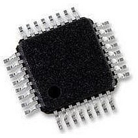
AT89C5115-RATUM Atmel, AT89C5115-RATUM Datasheet - Page 84

AT89C5115-RATUM
Manufacturer Part Number
AT89C5115-RATUM
Description
IC 8051 MCU FLASH 16K 32VQFP
Manufacturer
Atmel
Series
89Cr
Datasheet
1.T89C5115-RATIM.pdf
(113 pages)
Specifications of AT89C5115-RATUM
Core Processor
8051
Core Size
8-Bit
Speed
40MHz
Connectivity
UART/USART
Peripherals
POR, PWM, WDT
Number Of I /o
20
Program Memory Size
16KB (16K x 8)
Program Memory Type
FLASH
Eeprom Size
2K x 8
Ram Size
512 x 8
Voltage - Supply (vcc/vdd)
3 V ~ 5.5 V
Data Converters
A/D 8x10b
Oscillator Type
External
Operating Temperature
-40°C ~ 85°C
Package / Case
32-TQFP, 32-VQFP
Processor Series
AT89x
Core
8051
Data Bus Width
8 bit
Data Ram Size
512 B
Interface Type
UART
Maximum Clock Frequency
40 MHz
Number Of Programmable I/os
20
Number Of Timers
2
Operating Supply Voltage
3 V to 5.5 V
Maximum Operating Temperature
+ 85 C
Mounting Style
SMD/SMT
3rd Party Development Tools
PK51, CA51, A51, ULINK2
Development Tools By Supplier
CANADAPT28
Minimum Operating Temperature
- 40 C
On-chip Adc
10 bit, 8 Channel
Package
32VQFP
Device Core
8051
Family Name
89C
Maximum Speed
40 MHz
For Use With
AT89OCD-01 - USB EMULATOR FOR AT8XC51 MCU
Lead Free Status / RoHS Status
Lead free / RoHS Compliant
Available stocks
Company
Part Number
Manufacturer
Quantity
Price
Figure 38. ADC Description
Figure 39. Timing Diagram
Note:
ADC Converter
Operation
84
Tsetup min, see the AC Parameter for A/D conversion.
Tconv = 11 clock ADC = 1sample and hold + 10-bit conversion
The user must ensure that Tsetup time between setting ADEN and the start of the first conversion.
AN0/P1.0
AN1/P1.1
AN2/P1.2
AN3/P1.3
AN4/P1.4
AN5/P1.5
AN6/P1.6
AN7/P1.7
AT89C5115
ADEOC
ADSST
ADEN
CLOCK
CLK
ADC
ADCON.2
SCH2
000
001
010
011
100
101
110
111
T
SETUP
ADCON.1
SCH1
Figure 39 shows the timing diagram of a complete conversion. For simplicity, the figure
depicts the waveforms in idealized form and do not provide precise timing information.
For ADC characteristics and timing parameters refer to the section “AC Characteristics”
of this datasheet.
A start of single A/D conversion is triggered by setting bit ADSST (ADCON.3).
After completion of the A/D conversion, the ADSST bit is cleared by hardware.
The end-of-conversion flag ADEOC (ADCON.4) is set when the value of conversion is
available in ADDH and ADDL, it must be cleared by software. If the bit EADC (IEN1.1) is
set, an interrupt occur when flag ADEOC is set (See Figure 41). Clear this flag for re-
arming the interrupt.
Note:
ADCON.5
Sample and Hold
ADEN
CONTROL
ADCON.0
SCH0
Always leave Tsetup time before starting a conversion unless ADEN is permanently high.
In this case one should wait Tsetup only before the first conversion
Rai
Cai
ADCON.3
ADSST
AVSS
ADCIN
+
-
T
CONV
VAREF
ADCON.4
ADEOC
R/2R DAC
VAGND
SAR
EADC
IEN1.1
10
8
2
ADDH
ADDL
ADC
Interrupt
Request
4128G–8051–02/08


