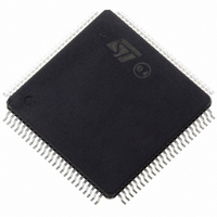
STR710FZ1T6 STMicroelectronics, STR710FZ1T6 Datasheet - Page 20

STR710FZ1T6
Manufacturer Part Number
STR710FZ1T6
Description
IC MCU ARM7 TDMI 128K 144TQFP
Manufacturer
STMicroelectronics
Series
STR7r
Datasheet
1.RLINK-ST.pdf
(78 pages)
Specifications of STR710FZ1T6
Core Processor
ARM7
Core Size
32-Bit
Speed
66MHz
Connectivity
CAN, EBI/EMI, HDLC, I²C, SmartCard, SPI, UART/USART, USB
Peripherals
PWM, WDT
Number Of I /o
48
Program Memory Size
128KB (128K x 8 + 16K)
Program Memory Type
FLASH
Ram Size
32K x 8
Voltage - Supply (vcc/vdd)
3 V ~ 3.6 V
Data Converters
A/D 4x12b
Oscillator Type
Internal
Operating Temperature
-40°C ~ 85°C
Package / Case
144-TQFP, 144-VQFP
Processor Series
STR710x
Core
ARM7TDMI
Data Bus Width
32 bit
Data Ram Size
32 KB
Interface Type
CAN, EMI, USB
Maximum Clock Frequency
16 MHz
Number Of Programmable I/os
48
Number Of Timers
5 x 16 bit
Operating Supply Voltage
3 V to 3.6 V
Maximum Operating Temperature
+ 85 C
Mounting Style
SMD/SMT
3rd Party Development Tools
EWARM, EWARM-BL, MCBSTR7, MDK-ARM, RL-ARM, ULINK2
Development Tools By Supplier
STR710-SK/HIT, STR711-SK/IAR, STR712-SK/IAR, STR71X-SK/RAIS, STX-PRO/RAIS, STX-RLINK, STR79-RVDK/CPP, STR79-RVDK, STR79-RVDK/UPG
Minimum Operating Temperature
- 40 C
On-chip Adc
12 bit
For Use With
MCBSTR7UME - MCBSTR7 + ULINK-ME DEV KITMCBSTR7 - BOARD EVAL STM STR71X SERIES497-5046 - KIT TOOL FOR ST7/UPSD/STR7 MCU497-4516 - BOARD EVAL FOR STR71X SER MCU
Lead Free Status / RoHS Status
Lead free / RoHS Compliant
Eeprom Size
-
Lead Free Status / Rohs Status
Details
Other names
497-4510
Available stocks
Company
Part Number
Manufacturer
Quantity
Price
Company:
Part Number:
STR710FZ1T6
Manufacturer:
STMicroelectronics
Quantity:
10 000
System architecture
Table 4.
20/78
143
144
Pin n°
C4
B3
P0.8/U0.RX/
U0.TX
P0.9/U0.TX/
BOOT.0
STR710 pin description
1. The Reset configuration of the I/O Ports is IPUPD (input pull-up/pull down). Refer to
2. In reset state, these pins configured as Input PU/PD with weak pull-up enabled. They must be configured
3. In reset state, these pins configured as Input PU/PD with weak pull-down enabled to output Address
4. V
5. During the reset phase, these pins are in input pull-up state. When reset is released, they are configured as
6. During the reset phase, these pins are in input pull-up state. When reset is released, they are configured as
7. During the reset phase, these pins are in input pull-down state. When reset is released, they are configured
8. During the reset phase, this pin is in input floating state. When reset is released, it is configured as Output
Pin name
The Port bit configuration at reset is PC0=1, PC1=1, PC2=0. The port data register bit (PD) value depends
on the pu/pd column which specifies whether the pull-up or pull-down is enabled at reset
by software as Alternate Function (see
External Memory Interface.
0x0000 0000 using the External Memory Interface. To access memory banks greater than 1Mbyte, they
need to be configured by software as Alternate Function (see
page
Output Push-Pull.
Hi-Z.
as Output Push-Pull.
Push-Pull.
33IO-PLL
29).
and V
I/O pd C
I/O pd C
33
are internally connected. V
Input
T
T
X 4mA T
4mA X
Output
Table 8: Port bit configuration table on page
SSIO-PLL
X
and V
Note: This pin may be used for single wire UART
(half duplex) if programmed as Alternate Function
Output. The pin will be tri-stated except when
UART transmission is in progress
function
Port 0.8
Port 0.9
reset)
(after
Main
SS
Table 8: Port bit configuration table on
are internally connected.
UART0:
Receive Data
input
Select Boot
Configuration
input
Alternate function
29) to be used by the
Table 8 on page
UART0: Transmit
data output.
UART0: Transmit
data output
STR71xF
29.


