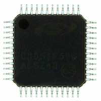
C8051F505-IQ Silicon Laboratories Inc, C8051F505-IQ Datasheet - Page 181

C8051F505-IQ
Manufacturer Part Number
C8051F505-IQ
Description
IC 8051 MCU 32K FLASH 48-QFP
Manufacturer
Silicon Laboratories Inc
Series
C8051F50xr
Specifications of C8051F505-IQ
Program Memory Type
FLASH
Program Memory Size
32KB (32K x 8)
Package / Case
48-QFP
Mfg Application Notes
LIN Bootloader AppNote
Core Processor
8051
Core Size
8-Bit
Speed
50MHz
Connectivity
EBI/EMI, SMBus (2-Wire/I²C), SPI, UART/USART
Peripherals
POR, PWM, Temp Sensor, WDT
Number Of I /o
40
Ram Size
4.25K x 8
Voltage - Supply (vcc/vdd)
1.8 V ~ 5.25 V
Data Converters
A/D 32x12b
Oscillator Type
Internal
Operating Temperature
-40°C ~ 125°C
Processor Series
C8051F5x
Core
8051
Data Bus Width
8 bit
Data Ram Size
4.25 KB
Interface Type
I2C/SPI/UART
Maximum Clock Frequency
50 MHz
Number Of Programmable I/os
40
Number Of Timers
4
Maximum Operating Temperature
+ 125 C
Mounting Style
SMD/SMT
3rd Party Development Tools
PK51, CA51, A51, ULINK2
Development Tools By Supplier
C8051F500DK
Minimum Operating Temperature
- 40 C
On-chip Adc
32-ch x 12-bit
Package
48PQFP
Device Core
8051
Family Name
C8051F50x
Maximum Speed
50 MHz
Operating Supply Voltage
2.5|3.3|5 V
Lead Free Status / RoHS Status
Lead free / RoHS Compliant
For Use With
336-1527 - KIT DEV FOR C8051F50X
Eeprom Size
-
Lead Free Status / Rohs Status
Lead free / RoHS Compliant
Other names
336-1520
Available stocks
Company
Part Number
Manufacturer
Quantity
Price
Company:
Part Number:
C8051F505-IQ
Manufacturer:
SLB
Quantity:
590
Company:
Part Number:
C8051F505-IQ
Manufacturer:
Silicon Laboratories Inc
Quantity:
10 000
Company:
Part Number:
C8051F505-IQR
Manufacturer:
Silicon Laboratories Inc
Quantity:
10 000
- Current page: 181 of 312
- Download datasheet (3Mb)
Registers XBR0, XBR1, and XBR2 are used to assign the digital I/O resources to the physical I/O Port
pins. Note that when the SMBus is selected, the Crossbar assigns both pins associated with the SMBus
(SDA and SCL); and similarly when the UART, CAN or LIN are selected, the Crossbar assigns both pins
associated with the peripheral (TX and RX). UART0 pin assignments are fixed for bootloading purposes:
UART TX0 is always assigned to P0.4; UART RX0 is always assigned to P0.5. CAN0 pin assignments are
fixed to P0.6 for CAN_TX and P0.7 for CAN_RX. Standard Port I/Os appear contiguously after the priori-
tized functions have been assigned.
Important Note: The SPI can be operated in either 3-wire or 4-wire modes, pending the state of the
NSSMD1–NSSMD0 bits in register SPI0CN. According to the SPI mode, the NSS signal may or may not
be routed to a Port pin.
As an example configuration, if CAN0, SPI0 in 4-wire mode, and PCA0 Modules 0, 1, and 2 are enabled on
the crossbar with P0.1, P0.2, and P0.5 skipped, the registers should be set as follows: XBR0 = 0x06
(CAN0 and SPI0 enabled), XBR1 = 0x0C (PCA0 modules 0, 1, and 2 enabled), XBR2 = 0x40 (Crossbar
enabled), and P0SKIP = 0x26 (P0.1, P0.2, and P0.5 skipped). The resulting crossbar would look as shown
in Figure 20.4.
Port
Special
Function
Signals
PIN I/O
UART_TX
UART_RX
CAN_TX
CAN_RX
SCK
MISO
MOSI
NSS
SDA
SCL
CP0
CP0A
CP1
CP1A
SYSCLK
CEX0
CEX1
CEX2
CEX3
CEX4
CEX5
ECI
T0
T1
LIN_TX
LIN_RX
0 1 2 3 4 5 6 7 0 1 2 3 4 5 6 7 0 1 2 3 4 5 6 7 0 1 2 3 4 5 6 7 0 1 2 3 4 5 6 7
P0
Figure 20.3. Peripheral Availability on Port I/O Pins
P1
Rev. 1.2
P2
available on the 48-pin
C8051F50x/F51x
P3.1-P3.7, P4.0 only
and 40-pin packages
P3
available on the 48-
P4.1-P4.7 only
pin packages
P4
181
Related parts for C8051F505-IQ
Image
Part Number
Description
Manufacturer
Datasheet
Request
R
Part Number:
Description:
SMD/C°/SINGLE-ENDED OUTPUT SILICON OSCILLATOR
Manufacturer:
Silicon Laboratories Inc
Part Number:
Description:
Manufacturer:
Silicon Laboratories Inc
Datasheet:
Part Number:
Description:
N/A N/A/SI4010 AES KEYFOB DEMO WITH LCD RX
Manufacturer:
Silicon Laboratories Inc
Datasheet:
Part Number:
Description:
N/A N/A/SI4010 SIMPLIFIED KEY FOB DEMO WITH LED RX
Manufacturer:
Silicon Laboratories Inc
Datasheet:
Part Number:
Description:
N/A/-40 TO 85 OC/EZLINK MODULE; F930/4432 HIGH BAND (REV E/B1)
Manufacturer:
Silicon Laboratories Inc
Part Number:
Description:
EZLink Module; F930/4432 Low Band (rev e/B1)
Manufacturer:
Silicon Laboratories Inc
Part Number:
Description:
I°/4460 10 DBM RADIO TEST CARD 434 MHZ
Manufacturer:
Silicon Laboratories Inc
Part Number:
Description:
I°/4461 14 DBM RADIO TEST CARD 868 MHZ
Manufacturer:
Silicon Laboratories Inc
Part Number:
Description:
I°/4463 20 DBM RFSWITCH RADIO TEST CARD 460 MHZ
Manufacturer:
Silicon Laboratories Inc
Part Number:
Description:
I°/4463 20 DBM RADIO TEST CARD 868 MHZ
Manufacturer:
Silicon Laboratories Inc
Part Number:
Description:
I°/4463 27 DBM RADIO TEST CARD 868 MHZ
Manufacturer:
Silicon Laboratories Inc
Part Number:
Description:
I°/4463 SKYWORKS 30 DBM RADIO TEST CARD 915 MHZ
Manufacturer:
Silicon Laboratories Inc
Part Number:
Description:
N/A N/A/-40 TO 85 OC/4463 RFMD 30 DBM RADIO TEST CARD 915 MHZ
Manufacturer:
Silicon Laboratories Inc
Part Number:
Description:
I°/4463 20 DBM RADIO TEST CARD 169 MHZ
Manufacturer:
Silicon Laboratories Inc


