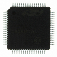
C8051F702-GQ Silicon Laboratories Inc, C8051F702-GQ Datasheet - Page 57

C8051F702-GQ
Manufacturer Part Number
C8051F702-GQ
Description
IC 8051 MCU 16K FLASH 64-TQFP
Manufacturer
Silicon Laboratories Inc
Series
C8051F70xr
Specifications of C8051F702-GQ
Program Memory Type
FLASH
Program Memory Size
16KB (16K x 8)
Package / Case
64-TQFP, 64-VQFP
Core Processor
8051
Core Size
8-Bit
Speed
25MHz
Connectivity
EBI/EMI, SMBus (2-Wire/I²C), SPI, UART/USART
Peripherals
Cap Sense, POR, PWM, Temp Sensor, WDT
Number Of I /o
54
Ram Size
512 x 8
Voltage - Supply (vcc/vdd)
1.8 V ~ 3.6 V
Data Converters
A/D 16x10b
Oscillator Type
Internal
Operating Temperature
-40°C ~ 85°C
Processor Series
C8051F7x
Core
8051
Data Bus Width
8 bit
Data Ram Size
512 B
Interface Type
I2C, SPI, UART
Maximum Clock Frequency
25 MHz
Number Of Programmable I/os
54
Number Of Timers
4 x 16 bit
Operating Supply Voltage
1.8 V to 3.3 V
Maximum Operating Temperature
+ 85 C
Mounting Style
SMD/SMT
3rd Party Development Tools
PK51, CA51, A51, ULINK2
Development Tools By Supplier
C8051F700DK
Minimum Operating Temperature
- 40 C
On-chip Adc
10 bit, 16 Channel
Lead Free Status / RoHS Status
Lead free / RoHS Compliant
For Use With
336-1635 - DEV KIT FOR C8051F700
Eeprom Size
-
Lead Free Status / Rohs Status
Lead free / RoHS Compliant
Other names
336-1608
Available stocks
Company
Part Number
Manufacturer
Quantity
Price
Company:
Part Number:
C8051F702-GQ
Manufacturer:
Silicon Laboratories Inc
Quantity:
10 000
Company:
Part Number:
C8051F702-GQR
Manufacturer:
Silicon Laboratories Inc
Quantity:
10 000
- Current page: 57 of 306
- Download datasheet (2Mb)
10.3.2. Tracking Modes
The AD0TM bit in register ADC0CN enables "delayed conversions", and will delay the actual conversion
start by three SAR clock cycles, during which time the ADC will continue to track the input. If AD0TM is left
at logic 0, a conversion will begin immediately, without the extra tracking time. For internal start-of-conver-
sion sources, the ADC will track anytime it is not performing a conversion. When the CNVSTR signal is
used to initiate conversions, ADC0 will track either when AD0TM is logic 1, or when AD0TM is logic 0 and
CNVSTR is held low. See Figure 10.2 for track and convert timing details. Delayed conversion mode is
useful when AMUX settings are frequently changed, due to the settling time requirements described in
Section “10.3.3. Settling Time Requirements” on page 58.
Timer 0, Timer 2, Timer 1 Overflow
(AD0CM[2:0]=000, 001, 010, 011)
Write '1' to AD0BUSY,
Figure 10.2. 10-Bit ADC Track and Conversion Example Timing
(AD0CM[2:0]=1xx)
SAR Clocks
AD0TM=1
AD0TM=0
AD0TM=1
AD0TM=0
CNVSTR
Clocks
Clocks
Clocks
SAR
SAR
SAR
N/C
Track or
Convert
A. ADC Timing for External Trigger Source
B. ADC Timing for Internal Trigger Source
Track
Track
Track
1 2 3 4 5 6 7 8 9 10 11 12 13 14 15* 16 17
1 2 3 4 5 6 7 8 9 10 11 12* 13 14
Rev. 1.0
1 2 3 4 5 6 7 8 9 10 11 12 13 14 15* 16 17
1 2 3 4 5 6 7 8 9 10 11 12* 13 14
Convert
Convert
*Conversion Ends at rising edge of 15
*Conversion Ends at rising edge of 12
*Conversion Ends at rising edge of 15
*Conversion Ends at rising edge of 12
Convert
Convert
C8051F70x/71x
th
th
th
clock in 8-bit Mode
th
clock in 8-bit Mode
clock in 8-bit Mode
Track
clock in 8-bit Mode
N/C
Track
Track
57
Related parts for C8051F702-GQ
Image
Part Number
Description
Manufacturer
Datasheet
Request
R
Part Number:
Description:
SMD/C°/SINGLE-ENDED OUTPUT SILICON OSCILLATOR
Manufacturer:
Silicon Laboratories Inc
Part Number:
Description:
Manufacturer:
Silicon Laboratories Inc
Datasheet:
Part Number:
Description:
N/A N/A/SI4010 AES KEYFOB DEMO WITH LCD RX
Manufacturer:
Silicon Laboratories Inc
Datasheet:
Part Number:
Description:
N/A N/A/SI4010 SIMPLIFIED KEY FOB DEMO WITH LED RX
Manufacturer:
Silicon Laboratories Inc
Datasheet:
Part Number:
Description:
N/A/-40 TO 85 OC/EZLINK MODULE; F930/4432 HIGH BAND (REV E/B1)
Manufacturer:
Silicon Laboratories Inc
Part Number:
Description:
EZLink Module; F930/4432 Low Band (rev e/B1)
Manufacturer:
Silicon Laboratories Inc
Part Number:
Description:
I°/4460 10 DBM RADIO TEST CARD 434 MHZ
Manufacturer:
Silicon Laboratories Inc
Part Number:
Description:
I°/4461 14 DBM RADIO TEST CARD 868 MHZ
Manufacturer:
Silicon Laboratories Inc
Part Number:
Description:
I°/4463 20 DBM RFSWITCH RADIO TEST CARD 460 MHZ
Manufacturer:
Silicon Laboratories Inc
Part Number:
Description:
I°/4463 20 DBM RADIO TEST CARD 868 MHZ
Manufacturer:
Silicon Laboratories Inc
Part Number:
Description:
I°/4463 27 DBM RADIO TEST CARD 868 MHZ
Manufacturer:
Silicon Laboratories Inc
Part Number:
Description:
I°/4463 SKYWORKS 30 DBM RADIO TEST CARD 915 MHZ
Manufacturer:
Silicon Laboratories Inc
Part Number:
Description:
N/A N/A/-40 TO 85 OC/4463 RFMD 30 DBM RADIO TEST CARD 915 MHZ
Manufacturer:
Silicon Laboratories Inc
Part Number:
Description:
I°/4463 20 DBM RADIO TEST CARD 169 MHZ
Manufacturer:
Silicon Laboratories Inc


