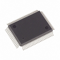
DS5002FPM-16+ Maxim Integrated Products, DS5002FPM-16+ Datasheet

DS5002FPM-16+
Specifications of DS5002FPM-16+
Related parts for DS5002FPM-16+
DS5002FPM-16+ Summary of contents
Page 1
... Power-Fail Reset Early Warning Power-Fail Interrupt Watchdog Timer ORDERING INFORMATION 64 P2.6/A14 63 CE3 62 CE4 61 PART BD3 60 P2.5/A13 59 BD2 58 P2.4/A12 DS5002FPM-16 57 BD1 56 DS5002FPM-16+ P2.3/A11 55 BD0 DS5002FMN-16 54 VLI DS5002FMN-16+ 53 SDI 52 GND 51 + Denotes a Pb-free/RoHS-compliant device. P2.2/A10 50 P2.1/A9 49 P2.0/A8 Selector Guide appears at end of data sheet. 48 XTAL1 47 ...
Page 2
ELECTRICAL SPECIFICATIONS The DS5002FP adheres to all AC and DC electrical specifications published for the DS5001FP. ABSOLUTE MAXIMUM RATINGS Voltage Range on Any Pin Relative to Ground……………………………………………………….-0. Voltage Range on V Relative to Ground……………………………………………………………………-0.3V to +6.0V CC Operating ...
Page 3
DC CHARACTERISTICS (continued ±10 0°C to +70°C.)** CC A PARAMETER Lithium Supply Voltage Operating Current at 16MHz Idle Mode Current at 12MHz Stop Mode Current Pin Capacitance Output Supply Voltage (V ) CCO Output Supply ...
Page 4
AC CHARACTERISTICS—EXPANDED BUS MODE TIMING SPECIFICATIONS ( ±10 0°C to +70°C PARAMETER 1 Oscillator Frequency 2 ALE Pulse Width 3 Address Valid to ALE Low 4 Address Hold After ALE Low 14 RD ...
Page 5
Figure 2. Expanded Data Memory Write Cycle AC CHARACTERISTICS—EXTERNAL CLOCK DRIVE ( ± 10 0°C to +70°C PARAMETER 28 External Clock High Time 29 External Clock Low Time 30 External Clock Rise Time ...
Page 6
AC CHARACTERISTICS—POWER CYCLE TIME ( ±10 0°C to +70°C PARAMETER 32 Slew Rate from CCMIN 33 Crystal Startup Time 34 Power-on Reset Delay Figure 4. Power Cycle Timing (Figure 4) ...
Page 7
AC CHARACTERISTICS—SERIAL PORT TIMING, MODE ±10 0°C to +70°C PARAMETER 35 Serial Port Clock Cycle Time 36 Output Data Setup to Rising Clock Edge 37 Output Data Hold after Rising Clock ...
Page 8
AC CHARACTERISTICS—BYTE-WIDE ADDRESS/DATA BUS TIMING ( ±10 0°C to +70°C PARAMETER Delay to Byte-Wide Address Valid from CE1 , 40 CE2 , or CE1N Low During Op Code Fetch Pulse Width of CE ...
Page 9
RPC AC CHARACTERISTICS, DBB READ ( ±10 0°C to +70°C PARAMETER Setup Hold After Pulse Width ...
Page 10
Figure 7. RPC Timing Mode ...
Page 11
PIN DESCRIPTION PIN NAME 11 General-Purpose I/O Port 0. This port is open-drain and cannot drive a logic 1. It requires 1, 79, 77, P0.0–P0.7 external pullups. Port 0 is also the multiplexed expanded address/data bus. When ...
Page 12
PIN NAME Active-Low Chip Enable 4. This chip enable is provided to access a fourth 32k block of CE4 62 memory. It connects to the chip-enable input of one SRAM. When MSEL = 0, this signal is unused. CE4 is ...
Page 13
DETAILED DESCRIPTION The DS5002FP implements a security system that is an improved version of its predecessor, the DS5000FP. Like the DS5000FP, the DS5002FP loads and executes application software in encrypted form 128kB of standard SRAM can be accessed ...
Page 14
Figure 8. Block Diagram ...
Page 15
SECURE OPERATION OVERVIEW The DS5002FP incorporates encryption of the activity on its byte-wide address/data bus to prevent unauthorized access to the program and data information contained in the NV RAM. Loading an application program in this manner is performed by ...
Page 16
Figure 9. Security Circuitry The address encryptor translates each “logical” address, i.e., the normal sequence of addresses that are generated in the logical flow of program execution, into an encrypted address (or “physical” address) at which the byte is actually ...
Page 17
DUMMY READ CYCLES Like the DS5000FP, the DS5002FP generates a “dummy” read access cycle to non-sequential addresses in external RAM memory whenever ...
Page 18
... V TOP LAYER COATING The DS5002FPM is provided with a special top-layer coating that is designed to prevent a probe attack. This coating is implemented with second-layer metal added through special processing of the microcontroller die. This additional layer is not a simple sheet of metal, but rather a complex layout that is interwoven with power and ground, which are in turn connected to logic for the encryption key and the security lock ...
Page 19
Table 1. Serial Bootstrap Loader Commands COMMAND C Return CRC-16 of the program/data NV RAM D Dump Intel Hex file F Fill program/data NV RAM G Get data from P1, P2, and P3 I N/A on the DS5002FP L Load ...
Page 20
The memory map and its controls are covered in detail in the Secure Microcontroller User’s Guide. Figure 10. Memory Map in Nonpartitionable Mode ( ...
Page 21
Figure 11. Memory Map In Partitionable Mode ( Figure 12. Memory Map with PES = ...
Page 22
Figure 13 illustrates a typical memory connection for a system using a 128kB SRAM. Note that in this configuration, both program and data are stored in a common RAM chip. SRAMs. The byte-wide address bus connects to the SRAM address ...
Page 23
Figure 14. Connection to 64k x 8 SRAM POWER MANAGEMENT The DS5002FP monitors V to provide power-fail reset, early warning power-fail interrupt, and switchover to CC lithium backup. It uses an internal bandgap reference in determining the switch points. These ...
Page 24
... SELECTOR GUIDE STANDARD Pb-FREE/RoHS PART COMPLIANT DS5002FP-16 DS5002FP-16+ DS5002FPM-16 DS5002FPM-16+ DS5002FP-16N DS5002FP-16N+ DS5002FMN-16 DS5002FMN-16+ PACKAGE INFORMATION (The package drawing(s) in this data sheet may not reflect the most current specifications. For the latest package outline information www.maxim-ic.com/DallasPackInfo.) MM DIM MIN A — A1 0. ...
Page 25
... Maxim/Dallas Semiconductor cannot assume responsibility for use of any circuitry other than circuitry entirely embodied in a Maxim/Dallas Semiconductor product. No circuit patent licenses are implied. Maxim/Dallas Semiconductor reserves the right to change the circuitry and specifications without notice at any time The Maxim logo is a registered trademark of Maxim Integrated Products, Inc. The Dallas logo is a registered trademark of Dallas Semiconductor Corporation. DESCRIPTION - 0 ...


